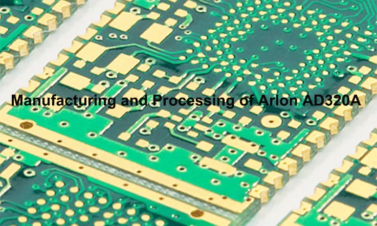
Arlon AD320A is a ceramic-filled PTFE laminate with a stable dielectric constant (3.20 ± 0.04) and low loss tangent (0.0032 @10 GHz), suited for RF, microwave, and high-frequency PCB builds. It supports consistent signal performance in multilayer applications such as base station antennas, medical imaging systems, radar, and satellite modules.
This document covers hybrid stackups with materials like FR4, RO4350B, and Megtron 6, as well as controlled impedance layering and EMI shielding methods. Comparative insights with RT/duroid 5880 highlight processing and cost-performance considerations.
Manufacturing capabilities—including laser-drilled microvias, high layer counts, and custom stackup support from JarnisTech—are detailed to reflect compatibility with diverse production needs. Tables and examples are included to support practical implementation and facilitate material selection across industrial and communication sectors.
Overview of Arlon AD320A PCB Laminate for High-Frequency Applications
Arlon AD320A PCB laminate has been engineered to meet the demands of high-frequency circuit applications where electrical stability, low signal loss, and thermal consistency are expected across multiple RF bands. The base material combines woven glass reinforcement, PTFE resin, and a controlled volume of ceramic fillers to achieve a dielectric system compatible with millimeter-wave and 5G systems.
Maintaining a stable dielectric constant and low dissipation factor across broad temperature and humidity conditions is fundamental to high-frequency PCB stackups. The material structure allows for predictable impedance in multilayer designs while also offering manufacturing flexibility. This makes AD320A laminate suitable for use in communication antennas, RF filters, microwave sensors, medical imaging devices, and power amplifiers operating at frequencies from 1 GHz to 40 GHz.
The following subsections describe the core characteristics of Arlon AD320A with respect to its material formulation and performance under electrical and thermal stress.
Electrical Parameters of Arlon AD320A PCB Materials
Arlon AD320A exhibits a well-balanced set of electrical properties targeted at low-loss high-frequency signal transmission.
●The dielectric constant (Dk) is maintained at 3.20 ± 0.04, measured at 10 GHz, providing consistent impedance control across multilayer structures.
●The dissipation factor (Df) is rated at 0.0032 at 10 GHz, resulting in low insertion loss across wideband frequencies.
●Dielectric properties remain stable across operating temperatures ranging from –40°C to +150°C, which supports design consistency in thermal cycling environments.
These parameters enable signal paths to maintain phase linearity and impedance uniformity across applications in 5G base stations, phased-array radar modules, and industrial high-frequency controllers.
Processing Development of the Arlon AD Series Laminate Technology
The Arlon AD laminate series has been progressively refined to align with the demands of high-frequency multilayer PCB processing.
●AD320A integrates a micro-dispersed ceramic filler system, improving the uniformity of electrical characteristics across panel surfaces compared to earlier AD-series variants such as AD255C.
●The Z-axis coefficient of thermal expansion (CTE) is below 40 ppm/°C, enhancing plated through-hole reliability during multiple lamination cycles and reflow processes.
●High peel strength between copper and laminate layers is maintained even after thermal stress, ensuring interlayer adhesion in both double-sided and multilayer RF designs.
This evolution supports volume manufacturing of advanced boards where mechanical consistency must align with controlled electrical behavior.
Low-Loss Stability Across 5G, IoT, and mmWave Frequencies
Signal integrity in wideband RF and mmWave environments depends heavily on consistent dielectric performance across all transmission layers.
●Insertion loss remains low up to 40 GHz, making the material applicable in 5G beamforming modules, high-speed connectors, and mmWave backhaul units.
●Stable dielectric constant across frequency helps maintain impedance consistency and supports accurate phase alignment in IoT gateway modules and RF switch matrices.
●The material shows minimal change in dissipation under moisture or environmental stress, offering stability for outdoor and automotive-grade wireless applications.
These characteristics provide confidence when used in high-density RF boards where stable electrical performance must be maintained through various deployment conditions.
Breakdown of Arlon AD320A PCB Materials and Structure
Understanding the internal structure and composition of Arlon AD320A laminates allows for more predictable electrical behavior and better thermal management in RF and microwave printed circuit boards. This section provides a closer look at the substrate composition, cladding options, and heat-related properties.
PTFE-Ceramic Composite Base Layer
Arlon AD320A utilizes a proprietary blend of polytetrafluoroethylene (PTFE) and ceramic fillers, providing balanced electrical and mechanical behavior across high-frequency signal paths.
Dielectric Behavior and Mechanical Stability-
●The material exhibits a dielectric constant (Dk) of 3.20 ±0.04 at 10 GHz (IPC-TM-650 2.5.5.5), delivering low dispersion characteristics over wideband frequency operations.
●Ceramic reinforcement improves dimensional stability and minimizes material movement during multilayer lamination or reflow exposure.
●The low z-axis CTE supports better via reliability, especially in stacked microvia or hybrid multilayer constructions.
This formulation makes the laminate suitable for PCB layouts where tight phase alignment and low insertion loss are required, especially in phased array radar systems and mmWave transceivers.
Copper Cladding Types and Surface Finish Options
The selection of copper cladding and surface treatment directly influences circuit integrity, etch definition, and conductor loss.
Foil Types and Compatibility-
●Standard offerings include reverse-treated copper, electrodeposited (ED), and rolled annealed (RA) foils with ½ oz to 2 oz thicknesses.
●Reverse-treated copper enhances adhesion to the PTFE matrix and improves lamination performance in hybrid stackups.
●Surface options such as ENIG (Electroless Nickel Immersion Gold), OSP, and immersion silver are compatible for achieving better solderability in high-density RF modules.
In applications requiring tight impedance control and low conductor loss, the proper pairing of foil type and finish becomes necessary to maintain signal integrity without unexpected impedance drifts.
Thermal Conductivity and Heat Dissipation Properties
The thermal profile of AD320A is tailored for reliable function in RF power amplifiers, medical imaging hardware, and high-density telecom boards.
Managing Thermal Loads in RF Systems-
●The laminate features a thermal conductivity of 0.50 W/m·K, ensuring consistent heat spread without the need for additional metal inlays.
●With a Tg above 250°C and a decomposition temperature (Td) of >500°C, the laminate handles repeated soldering and high-temp curing cycles.
●The low moisture absorption (<0.05%) supports applications in humid environments or where condensation can’t be fully avoided.
Such attributes enable reliable system behavior across outdoor telecom systems and high-reliability industrial sensors.
Arlon AD320A vs Rogers and Other Microwave PCB Materials

High-frequency circuit board materials often dictate the performance boundaries of RF and microwave applications. When selecting substrates for systems requiring stable dielectric properties, low loss, and mechanical consistency, materials like Arlon AD320A and Rogers RT/duroid 5880 frequently enter the evaluation shortlist. This section breaks down comparative technical performance metrics, production-scale behavior, and use case suitability across widely applied microwave laminates. The following subsections offer a practical lens through which substrate selection can be fine-tuned for frequency stability, thermal management, and fabrication compatibility.
Comparative Analysis: AD320A vs Rogers RT/duroid 5880
A detailed evaluation of Arlon AD320A and Rogers RT/duroid 5880 reveals differences in dielectric behavior, thermal expansion, and processing adaptability.
Dielectric Properties and Frequency Response-
| Property | Arlon AD320A | Rogers RT/duroid 5880 |
| Dielectric Constant (10 GHz) | 3.20 ± 0.04 | 2.20 ± 0.02 |
| Dissipation Factor (10 GHz) | 0.0032 | 0.0009 |
| Thermal Coefficient of Dk | -160 ppm/°C | -125 ppm/°C |
●AD320A’s higher Dk supports more compact RF line design, particularly beneficial in multilayer setups where space is at a premium.
●RT/duroid 5880 exhibits lower loss tangent, supporting applications above 20 GHz where signal attenuation must be minimized.
●Processing temperatures and mechanical handling differ, with AD320A tolerating more aggressive lamination profiles.
Cost-Performance Ratio in Mid-Volume Production
While performance metrics provide clarity, mid-range production costs and yield consistency often drive laminate preference for telecom, radar, or satellite systems.
Fabrication Yield, Etch Definition, and Laminate Handling-
| Parameter | AD320A | RT/duroid 5880 |
| Standard Panel Size | 18″x24″ or 24″x36″ | 12″x18″ or 18″x24″ |
| Dimensional Stability (MD/CD) | ±0.05% | ±0.20% |
| Yield Loss in Sequential Lamination | <2% | 3%–5% (avg) |
●AD320A’s ceramic-filled structure enhances drill quality and reduces debris-related faults during backdrilling.
●Better panel utilization rates contribute to lower cost-per-board in larger-format fabrication.
●RT/duroid 5880 often demands tighter process windows and softer mechanical handling, raising costs in volume.
Selecting the Right High-Frequency Laminate
Selecting a substrate for high-frequency boards calls for a balance between electrical targets, mechanical tolerance, and availability in multilayer-compatible formats.
Use Case Mapping and Application Fit-
| Application Type | Recommended Substrate |
| Base station antennas (5–10 GHz) | Arlon AD320A |
| Millimeter-wave radar (>20 GHz) | Rogers RT/duroid 5880 |
| Satellite IF amplifiers | AD320A or hybrid stackups |
●AD320A shows stable dielectric behavior under mixed-layer stackups, especially when paired with FR4 or low-Df glass-reinforced cores.
●RT/duroid 5880 is more appropriate for ultra-low loss scenarios but often lacks rigidity for complex mechanical integration.
●Lead time and material sourcing favor AD320A in North American and European supply chains.
PCB Stackup and Layering Strategies for AD320A Designs
The structural configuration of multilayer PCBs using Arlon AD320A laminate directly influences impedance stability, interlayer isolation, and system-level electromagnetic performance. To address diverse integration demands across RF, mmWave, and mixed-signal domains, we often evaluate hybrid stackup combinations, dielectric alignment, and shielding techniques with precision.
Hybrid Stackups with FR4, RO4350B, or Megtron 6
When integrating AD320A into multilayer designs, hybrid stackups allow material optimization across electrical and thermal dimensions. FR4, RO4350B, and Megtron 6 are frequently paired to balance performance targets with manufacturability constraints.
Considerations:
●RO4350B serves as a compatible pairing for mid-frequency applications, offering controlled Dk (3.48) while maintaining fabrication consistency with AD320A.
●Megtron 6 enhances thermal reliability in dense stackups, particularly where interlayer resin flow control is necessary.
●FR4, while not preferred for RF paths, may be used in ground or mechanical layers to reduce cost in non-signal-carrying planes.
This combination strategy should be validated through simulation and cross-checked against thermal expansion and z-axis stability parameters to prevent via stress or pad cratering during reflow cycles.
Matching Dielectric Layers for Impedance Control
Precise impedance modeling is feasible only when dielectric layers across adjacent planes exhibit uniformity in Dk, thickness, and resin content. AD320A, with its Dk of 3.20 ± 0.04 at 10 GHz, offers a stable basis for impedance control in RF structures.
Key practices include:
●Maintain consistency between prepreg and core thickness across differential pairs.
●Evaluate resin content in bonding layers to mitigate z-axis expansion mismatch.
●Apply impedance modeling tools calibrated for RF substrates rather than FR4 assumptions.
Measurement-based validation using Time Domain Reflectometry (TDR) across manufactured coupons is recommended to fine-tune design tolerances. This ensures predictable performance across the full operating bandwidth.
Crosstalk and Isolation Techniques for RF Layers
Reducing electromagnetic coupling between signal traces supports channel consistency at high frequencies. With a low loss tangent (Df ≤ 0.0032 at 10 GHz), AD320A helps maintain signal amplitude over extended trace lengths, though physical layout continues to influence overall performance.
Engineering practices:
●Apply solid ground planes adjacent to RF layers to contain field propagation.
●Maintain trace-to-trace spacing at least 3x the trace width to reduce near-end and far-end crosstalk.
●Consider stripline over microstrip configurations for enhanced shielding, especially above 10 GHz.
Where shielding effectiveness is a priority, backdrilling, stitching vias, and strategic via fences should be included in layout planning. These structures suppress parasitic modes and enhance edge containment across the entire board footprint.
Advanced Arlon AD320A PCB Design for RF and Microwave
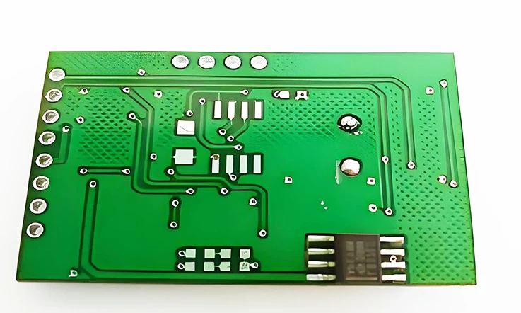
Working with Arlon AD320A laminates in high-frequency applications demands attention to electromagnetic behavior, dielectric uniformity, and mechanical reliability. The substrate’s Dk of 3.20 ±0.05 and low dissipation factor offer consistency in RF propagation, which can be leveraged in narrowband filters, phased-array modules, and mmWave transceivers. Layout optimization on this material is typically driven by impedance control, layer arrangement, and field confinement techniques.
Controlled Impedance Routing on AD320A Substrates
Consistent impedance across interconnects is a fundamental consideration when working with Arlon AD320A PCB design—especially in RF front-end modules and high-speed digital subsystems.
●Microstrip and stripline routing must account for the 3.20 Dk, which influences trace width and dielectric spacing; using standard equations may lead to mismatches if material anisotropy is ignored.
●Copper thickness uniformity and etch compensation during imaging directly impact impedance targets; it’s advised to simulate trace widths based on actual etch-back data rather than nominal specs.
●Embedded ground plane integrity should be prioritized to reduce reflection and phase shift—achievable by tight layer stacking and symmetrical configurations.
These techniques are often applied in controlled impedance PCBs operating between 1 GHz and 40 GHz, where phase consistency can influence RF system calibration.
Table 1: Typical Trace Widths for 50Ω Microstrip on AD320A (Dk = 3.20 ±0.04)
| Dielectric Thickness (mil) | Copper Weight (oz) | Target Impedance (Ω) | Calculated Trace Width (mil) |
| 5.0 | 0.5 | 50 | 11.8 |
| 8.0 | 1.0 | 50 | 15.6 |
| 10.0 | 1.0 | 50 | 18.3 |
Designing with Dk 3.20: Layout and Stackup Tips
The unique dielectric constant of Arlon AD320A PCB materials invites specific layout considerations, especially when building compact multilayer architectures.
●Multilayer stackups benefit from alternating low-Dk and copper-heavy prepreg layers, offering improved impedance control and thermal expansion matching.
●Isolation routing between RF lines should maintain ≥3x line width spacing to reduce coupling; for 50-ohm lines, this often translates to 15–20 mils depending on the stack height.
●Placement of decoupling capacitors near power-entry points on mixed-signal AD320A boards is advised to reduce broadband noise injection into RF domains.
These layout and stacking strategies are commonly used in IoT antennas, automotive radar, and medical imaging RF subsystems based on AD320A laminates.
Table 2: Example of 4-Layer Stackup Using AD320A
| Layer | Material | Thickness (mil) | Notes |
| L1 | Signal | — | Top layer, RF routing |
| — | AD320A Core | 10.0 | Dk = 3.20 ±0.05 |
| L2 | Ground Plane | — | Solid copper for shielding |
| — | Prepreg (filled) | 8.0 | Matched CTE, copper-heavy configuration |
| L3 | Power / Signal | — | Mixed-signal distribution |
| — | AD320A Core | 10.0 | Same as top for symmetry |
| L4 | Ground / Signal | — | Bottom routing / plane |
EM Simulation and SI/PI Analysis for High-Speed Designs
Simulating electrical behavior on AD320A substrates allows layout teams to avoid rework and prevent signal degradation, especially in environments exceeding 6 GHz.
●3D EM solvers (e.g., Ansys HFSS or CST Studio) help evaluate trace performance across stackup transitions and via arrays; using AD320A-specific Dk and Df profiles enhances accuracy.
●Signal integrity (SI) analysis should include S-parameters for insertion loss and return loss across the full operational bandwidth; this helps validate the consistency of transmission paths.
●Power integrity (PI) simulations for high-current rails on mixed-signal boards support the creation of low-impedance paths in configurations where AD320A is used alongside active components.
Table 3: Typical S-Parameter Results from AD320A-Based SI Simulation (10 GHz Bandwidth)
| Frequency (GHz) | Insertion Loss (dB) | Return Loss (dB) | Impedance Deviation (Ω) |
| 1 | -0.10 | -26 | ±1.2 |
| 5 | -0.28 | -20 | ±1.7 |
| 10 | -0.52 | -17 | ±2.1 |
Manufacturing Process Optimization for Arlon AD320A PCBs
Optimizing the manufacturing flow for Arlon AD320A PCBs demands a comprehensive understanding of how this ceramic-filled PTFE laminate interacts with high-frequency fabrication processes. From multilayer lamination to drill bit integrity and plasma activation, each variable can influence final board performance across applications such as medical imaging systems, satellite communications, and industrial radar modules.
Prepreg Compatibility and Multilayer Lamination Best Practices
Aligning Arlon AD320A PCB laminates with appropriate prepreg systems requires attention to thermal behavior and dimensional stability during lamination. Since AD320A features a dielectric constant (Dk) of 3.20 and low z-axis expansion, thermal excursions must be carefully controlled.
Lamination Considerations with Mixed Dielectric Systems
When Arlon AD320A is used in hybrid stackups with other prepregs or core materials:
●Use low-flow or no-flow prepregs with compatible melt viscosity and cure temperature profiles.
●Maintain lamination pressures between 250–350 psi, depending on stack height and copper density.
●Pre-bake all prepreg layers to eliminate residual moisture before lamination, particularly in high-layer-count boards.
Stackup planning should also consider resin bleed control, interlaminar adhesion, and z-axis CTE matching. Hybrid RF/microwave stackups incorporating AD320A with epoxy-based cores should prioritize thermal expansion balance to mitigate reliability degradation under thermal shock testing.
Plasma Surface Treatment for Enhanced Adhesion
Surface energy plays a direct role in copper adhesion to PTFE-based substrates. Due to the inherently low surface energy of AD320A, plasma treatment is a preferred technique for improving adhesion between laminate and inner copper layers, as well as soldermask or plating interfaces.
Process Guidelines for Uniform Plasma Activation-
●Deploy oxygen or argon plasma pre-treatment before multilayer lamination or metal deposition to elevate surface energy and remove residual processing films.
●Control chamber pressure between 200–600 mTorr, depending on surface area and feature density.
●Follow plasma cycles with nitrogen purge and low-temperature bake, typically at 110–130°C, to maintain surface activation without oxidation.
This process improves the mechanical bond without requiring aggressive chemical etching, making it suitable for applications in RF filter circuits, impedance-controlled backplanes, and mmWave phased arrays.
Bake Cycles, Drill Bit Wear, and Panel Flatness Control
Drilling and dimensional control with AD320A require refined process tuning, particularly at high layer counts or with tight mechanical tolerances. Material softness and filler loading can lead to burr formation or drill smear without appropriate controls.
Drilling & Post-Processing Best Practices-
●Use diamond-coated or micrograin carbide drill bits with high RPM and pecking cycles for hole diameters under 0.3 mm.
●Bake AD320A panels for 2–4 hours at 110–125°C before and after drilling to minimize moisture-induced warping and delamination.
●Maintain flatness below 0.1 mm per 500 mm of panel length using controlled cooling and uniform copper distribution in the layout.
These steps help maintain consistent plated-through-hole quality and panel yield during final test. For OEMs in the communications infrastructure field, where mmWave performance must meet defined thresholds, optimizing these steps supports signal fidelity and mechanical robustness.
Arlon AD320A PCB Manufacturing Considerations
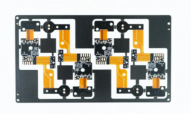
Manufacturing with Arlon AD320A PCB laminates requires well-defined process conditions due to the material’s composite nature. The blend of PTFE resin, ceramic fillers, and woven fiberglass affects every stage of fabrication—from lamination and drilling to desmear and final inspection. This section describes procedures frequently adopted by high-frequency PCB fabrication to manage dimensional precision, signal behavior, and mechanical durability. These methods apply to high-end applications including 5G communication modules, millimeter-wave automotive radar systems, industrial RF sensors, and medical RF imaging subsystems.
Lamination Parameters for AD320A PCB Laminates
Layer bonding with AD320A laminates must be handled with temperature, pressure, and timing strategies tailored to the material’s dielectric properties.
●Press temperature typically ranges from 185°C to 196°C (365°F to 385°F), held under vacuum for 60 to 90 minutes. This allows the PTFE resin to fully flow around glass and ceramic structures.
●Pressures between 275 and 350 psi are recommended, applied gradually with a ramp rate below 6°F/min to minimize trapped air and void formation.
●Cooling should take place under pressure until the stack temperature falls below 65°C (150°F), preventing delamination and resin pull-back.
These steps support uniform lamination of Arlon AD320A PCB materials in both single-layer and complex multilayer configurations, particularly where hybrid stackups are involved.
Drilling and Desmear in Arlon AD320A PCB Manufacturing
Mechanical processing of AD320A laminates presents challenges due to the combination of low resin melt point and high filler content.
●Recommended spindle speeds range from 300 to 350 surface feet per minute (SFM), with feed rates from 1.5 to 3.0 inches per minute (IPM), using undercut carbide drill bits for improved debris clearance.
●Desmear is best performed via plasma etching using oxygen and CF4 gases. This method modifies PTFE hole walls for enhanced metal adhesion during plating.
●Conventional permanganate desmear is generally avoided, as its chemical action has limited interaction with PTFE matrices.
These settings support the formation of clean via walls, a requirement in AD320A PCB manufacturing services involving high-density interconnects or high-frequency signal routing.
Quality Control in Arlon AD320A PCB Manufacturing Services
Process validation for AD320A PCB manufacturing goes well beyond visual inspection or basic electrical tests. Fabricators typically adopt comprehensive quality checks tailored for high-frequency applications.
●Cross-sectional analysis is used to measure layer thickness, resin coverage, and copper wall continuity in multilayer builds.
●S-parameter testing at 10 GHz or above helps verify insertion loss levels, comparing actual board data to simulation targets.
●Thermal stress testing—such as 288°C solder dip tests—ensures the laminate maintains structural stability across lead-free reflow cycles.
For production environments handling Arlon AD320A PCB materials, quality systems often include statistical process control and data logging for long-term trend analysis and traceability.
Applications of Arlon AD320A PCB in Medical and Communication Electronics
Arlon AD320A laminate is utilized in electronic platforms requiring controlled signal propagation, dielectric stability under thermal and moisture variation, and compatibility with industry-recognized processing requirements. Its performance characteristics position it as a suitable choice in areas such as medical diagnostics, wireless communication modules, and patient monitoring systems. This section examines its use from three technical perspectives: electromagnetic shielding characteristics, regulatory alignment processes, and RF performance stability across frequency ranges.
EMI Shielding Capabilities in Life-Sustaining Electronic Platforms
Electromagnetic interference (EMI) mitigation in high-frequency medical and communication systems depends on material composition, conductive layer selection, and substrate stability. AD320A, a ceramic-filled PTFE laminate, offers a relatively low dissipation factor and consistent dielectric behavior, which support high-frequency shielding without excessive signal degradation.
Application Insight-
In RF telemetry for clinical implants and medical imaging interfaces, susceptibility to EMI often limits usable bandwidth. AD320A supports field containment when paired with low-profile rolled annealed (RA) copper and ENIG finish. The following table illustrates shielding effectiveness across selected frequency bands:
| Frequency (GHz) | Shielding Effectiveness (dB) | Surface Finish |
| 2.4 | 56.3 | ENIG (0.1 µm Au) |
| 5.8 | 52.1 | Immersion Silver |
| 10.0 | 47.9 | Bare Copper (RA) |
Material consistency in high-frequency EMI environments contributes to predictable shielding outcomes. For manufacturers of EMI-sensitive devices, controlling loss and surface current behavior starts with selecting a stable substrate.
Regulatory Compliance for Medical Device PCBs
Compliance with standards such as UL94, IPC-4103, and RoHS is a prerequisite in medical electronics development. Arlon AD320A is UL94 V-0 rated and IPC-4103 Type II qualified, supporting traceable manufacturing processes and dielectric characterization compatible with FDA documentation practices.
Application Insight-
For defibrillator control units and ultrasound imaging boards, uniform dielectric values and full lot traceability can support successful regulatory submissions. AD320A’s material profile, including coefficient of thermal expansion (CTE) and dielectric constant across temperature sweeps, aligns with medical validation requirements. Moreover, its compatibility with biocompatible solder masks and lead-free surface finishes simplifies qualification processes.
Many manufacturers pursuing FDA or IEC 60601-1 compliance often include AD320A in baseline material qualification due to its measurable stability and conformity with flammability and toxicology thresholds.
Consistent RF Response Across Frequency Bands
Systems operating over multiple frequency ranges—from ISM to Ku-band—require laminates with limited dielectric drift and low phase delay variability. AD320A is designed with a controlled ceramic filler distribution to minimize Dk variation across both environmental and frequency-dependent stress.
Application Insight-
Medical telemetry devices and communication modules for base stations often require precise group delay and low insertion loss. AD320A exhibits <2% deviation in Dk between -40°C and +125°C. When used in 50-ohm microstrip configurations, its group delay remains consistent within ±0.05 ns across X- to Ku-band frequencies. The chart below shows measured delay trends in a 2-layer microstrip build:
| Frequency (GHz) | Group Delay (ns) | Dk Drift (Relative) |
| 2.45 | 1.23 | +0.9% |
| 5.80 | 1.19 | +1.1% |
| 10.00 | 1.17 | +1.8% |
Predictable frequency response enables reduced re-tuning effort across revisions of high-frequency designs.
Why Choose JarnisTech to Fabrication Your Arlon AD320A PCB?
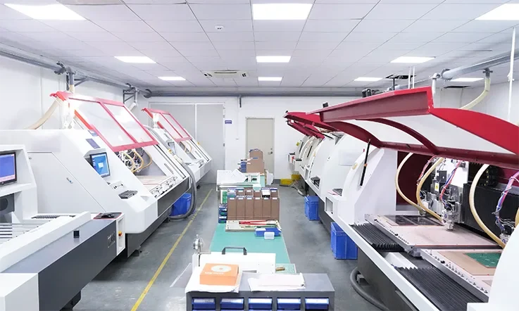
Selecting a PCB fabricator with experience in handling high-frequency laminates like Arlon AD320A directly influences the feasibility of applying this material to advanced systems. From controlled impedance routing to consistent z-axis dielectric behavior, the manufacturing process must align with stringent RF design constraints. JarnisTech maintains process capabilities tailored to the mechanical, thermal, and RF specifications of AD320A substrates, supporting both low-loss signal propagation and structural integrity across diverse stackups. The following sections outline specific service areas that enable practical customization using Arlon AD320A in RF, microwave, and mixed-signal PCB production.
Customization Capabilities in Arlon AD320A PCB Manufacturing Services
Arlon AD320A requires nuanced process adjustments that differ significantly from standard FR4 workflows. These include laminate pre-conditioning, low-residue etching, and fine-line imaging suitable for RF paths and ground shielding features. JarnisTech supports client-specified layouts through full in-house adaptation of lamination parameters, copper foil selection, and etch-back controls.
Application-Driven Customization Strategies-
●Support for mixed dielectric configurations integrating AD320A with RO4350B or FR4.
●Optimization of press cycles for high-aspect ratio PCBs.
●Customized copper weight and etch compensation per RF line width tables.
Table 1: Example of Prepreg/Copper Configuration for 4-Layer AD320A/FR4 Hybrid Stack
| Layer | Material | Copper (oz) | Dielectric Thickness (mil) |
| L1 | AD320A | 0.5 | 10 |
| L2 | FR4 Core | 1.0 | 40 |
| L3 | AD320A | 0.5 | 10 |
| L4 | FR4 Prepreg | 1.0 | 43 |
Laser Drilling and Microvia Design Options
With rising density in RF front-end and phased-array modules, microvia implementation becomes fundamental. AD320A exhibits a glass transition temperature that tolerates CO₂ laser ablation under controlled focus conditions. JarnisTech maintains process repeatability for stacked and staggered laser vias across multilayer builds.
Drilling Support Highlights-
●Compatibility with stacked microvias up to 3 layers deep.
●Minimum via diameter: 0.1 mm using UV or CO₂ laser methods.
●Via reliability validated through IST (Interconnect Stress Test) cycles.
Cross-sectional analysis of drilled microvias on AD320A reveals stable resin wall formation without signs of carbonization, supporting predictable behavior at microwave frequencies.
High-Layer-Count PCB Capabilities Using AD320A
Microwave modules integrated into communication satellites and military transceivers often require 8 to 20 layer PCBs, combining RF, power, and logic in a confined footprint. JarnisTech accommodates such builds with matched CTE planning and symmetrical stack balancing.
Layering and Warpage Control Practices-
●Max 20-layer fabrication with flatness ≤ 0.75% per IPC-TM-650.
●Thermal cycle pre-conditioning at 150°C for 2 hrs prior to lamination.
●Alignment accuracy within ±50 µm across stack height.
Custom Stackup and DFM Support from JarnisTech
Arlon AD320A’s dielectric constant and loss tangent must be matched across differential pairs and controlled impedance traces. JarnisTech offers DFM consultation based on client simulation data and provides real-time stackup modeling via Speedstack and Polar Si9000 tools.
DFM Integration Features-
●Pre-fabrication impedance simulation support based on transmission line structures.
●Stackup modeling for up to 12 dielectric layers including AD320A, RO4003C, or PTFE.
●Data package support in IPC-2581 or Gerber X2 for streamlined workflow.
FAQs – Arlon AD320A PCB Laminate
1.What is the typical copper peel strength of Arlon AD320A?
7.0 lb/in (1.23 N/mm) for 1 oz copper, tested per IPC-TM-650 2.4.8.
2.Is Arlon AD320A compatible with lead-free soldering processes?
Yes. With proper thermal management, it tolerates reflow up to 260°C.
3.Does AD320A support controlled depth milling?
Yes, the material can be processed using precision mechanical or laser depth-milling techniques.
4.What are the recommended storage conditions for AD320A prepreg and cores?
Store in a clean, dry area below 23°C with <50% RH; vacuum sealing is advised for extended shelf life
5.Can Arlon AD320A be bonded with fusion bonding methods?
No, it requires PTFE-compatible thermoset prepregs or bonding films.
6.Is AD320A suitable for embedded passive components?
Yes, its dimensional stability allows integration of embedded resistors or capacitors in multilayer stacks.
7.Does AD320A support sequential lamination?
Yes, with appropriate bonding films and bake cycles, sequential builds are feasible.
8.Can AD320A be combined with LCP or polyimide in hybrid boards?
Not recommended due to mismatch in z-axis expansion and bond interface chemistry.
9.How does AD320A perform in flexible or rigid-flex designs?
It’s not suitable for flex circuits due to its ceramic-filled PTFE structure.
10.What plating systems are compatible with AD320A for via reliability?
Direct metallization systems such as Blackhole® or Electroless Copper processes are compatible with proper surface prep.
Our services
Arlon PCB Laminate & Materials Series

