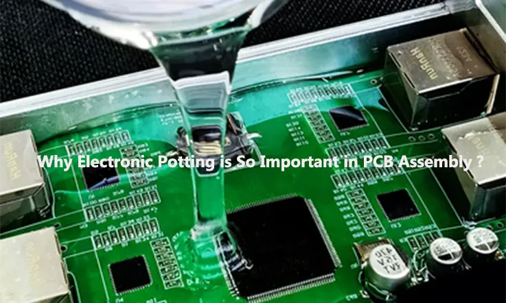
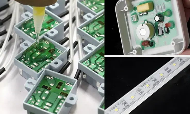
Electronic potting, also known as encapsulation or potting, is a process used to protect electronic components from environmental stress such as moisture, vibration, and shock. The process involves placing the electronic components into a potting material, which is then cured to create a hard, protective barrier around the components.
Electronic potting is commonly used in various industries, including aerospace, automotive, marine, and medical, to protect electronic components from harsh operating conditions. The process helps to increase the durability and reliability of electronic devices, ensuring they perform optimally and have a longer lifespan.
In this article, we will explore the electronic potting process, the materials used, and the benefits it provides. We will also discuss the different types of electronic potting materials available and the factors to consider when selecting the right potting material for a specific application.
What is Electronic Potting?
In the field of electronics, potting is a process that involves filling an entire electronic assembly with a solid or gelatinous compound to protect it against shock, vibration, and moisture. While the transition from mechanical to electronic solutions has reduced the wear and material fatigue associated with moving parts, solid-state technology still faces challenges that can impact its reliability.
One such challenge is the issue of moisture in electronics, which can lead to false alarms, faulty operation, micro-corrosion, and ultimately, component and system failure. Accelerated aging is another concern, resulting from air pockets, gaps, and exposure to corrosive agents. Although these issues can be addressed by using suitable enclosures to protect vulnerable components and systems, this can increase cost and add size and weight.
Potting offers an alternative solution to mechanical encapsulation. The process involves encapsulating electronic components in suitable enclosures and compounds, similar to stabilizing the root system of a plant by placing it in a pot and filling it with soil. This method provides protection against shock, vibration, moisture, and corrosive agents, ensuring that vulnerable electronic components remain unharmed.
How Does Electronics Potting Work?
Electronic potting is a process that involves encapsulating electronic components in a specialized container, typically made of epoxies, polyurethanes, or silicones. These materials have thermal insulation and adhesive structural properties that protect the electronics from harsh environmental conditions and physical damage.
Potting can be achieved by creating a mold or cast that is removed once the potting compound has hardened, or by dipping components into the compound to encapsulate them. This process is highly flexible and can be applied to specific high-risk parts and components or to complete boards and assemblies.
The advantages of potting electronics are numerous. Potting materials are available in a variety of formulations that address conductivity, electrical and thermal isolation, and protection against various environmental conditions and threats. This flexibility allows designers and manufacturers to choose the best materials for their specific application needs.
The Electronics Potting Process
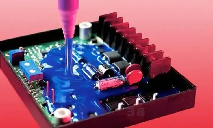
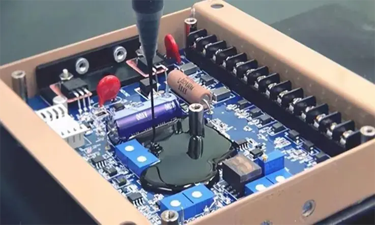
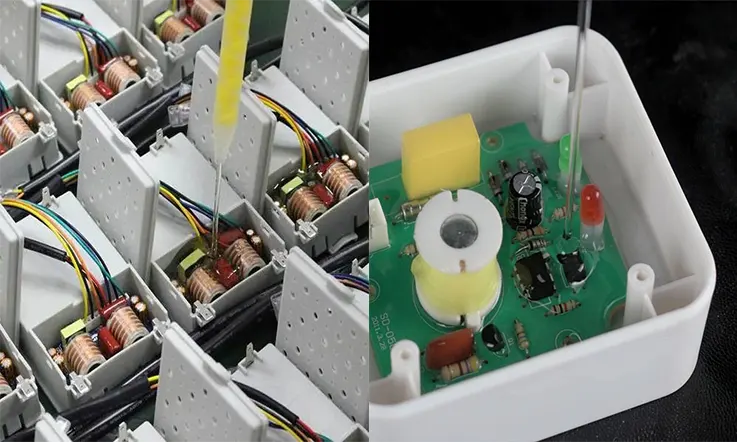
The electronics potting process is a method of protecting electronic components and devices from environmental factors such as moisture, vibration, and shock. Potting involves encapsulating the electronic components in a protective material, typically a thermosetting polymer, to create a durable and long-lasting seal.
The process typically involves the following steps:
1. Preparation: The electronic components are cleaned, dried, and prepared for potting.
2. Mixing: The potting material is mixed according to the manufacturer’s instructions. This may involve combining two or more components, such as a resin and hardener.
3. Potting: The mixed potting material is poured or injected into the enclosure or housing containing the electronic components. The potting material fills all the voids and covers the components completely.
4. Curing: The potting material is allowed to cure or harden, typically at room temperature or with the help of heat.
5. Finishing: After the potting material has cured, any excess material is trimmed or removed, and the electronic device is ready for use.
The potting material used can vary depending on the application and the desired properties. Common materials include epoxy resins, polyurethanes, and silicones. The material chosen should have good adhesion to the components and housing, provide a good seal, have good electrical properties, and be resistant to the expected environmental conditions.
The Benefits of Electronic Potting
Electronic potting is a highly effective method for protecting electronic devices and components, offering a range of benefits, including:
Environmental Protection: Potting materials act as a barrier against moisture, dust, dirt, and other environmental factors that can damage electronic components, ensuring optimal performance and longevity.
Durability Enhancement: Potting materials provide a protective layer around electronic components, making them more resistant to physical damage from vibration, impact, and shock, thereby increasing their durability.
Thermal Management Improvement: Many potting materials have excellent thermal conductivity properties, which can help to dissipate heat generated by electronic components, resulting in improved thermal management.
Increased Reliability: Potting helps to prevent corrosion and oxidation of electronic components, reducing the risk of failure and increasing device reliability.
Electrical Insulation Enhancement: Potting materials can enhance the electrical insulation properties of electronic components, reducing the risk of electrical shorts and other problems, thereby improving safety.
Customization Flexibility: Potting materials can be customized to meet specific design requirements, such as color, hardness, and flexibility, providing design flexibility to meet various application needs.
Overall, electronic potting is a valuable process for protecting electronic devices and components, and its benefits make it an essential consideration for many electronic design and manufacturing applications.
Electronic Potting Types
There are several methods of electronic potting, each with its own advantages and disadvantages. Here are some common electronic potting methods:
Manual potting: In this method, the potting material is poured or injected by hand into the enclosure or housing containing the electronic components. Manual potting is suitable for low-volume production runs or for prototyping, but it can be time-consuming and may not provide consistent coverage or quality.
Vacuum potting: In this method, the electronic components are placed in a vacuum chamber, and the potting material is injected under vacuum. This method helps to remove air bubbles and ensure complete coverage of the components, but it requires specialized equipment and can be expensive.
Pressure potting: In this method, the electronic components are placed in a pressure vessel, and the potting material is injected under pressure. Pressure potting helps to remove air bubbles and ensure complete coverage of the components, but it also requires specialized equipment and can be expensive.
Transfer potting: In this method, the potting material is poured into a potting tool or mold, and the electronic components are placed into the tool or mold. The potting material is then cured around the components. Transfer potting can provide consistent coverage and quality, but it requires specialized equipment and molds.
Injection molding: In this method, the potting material is injected into a mold containing the electronic components. The mold is then heated and cooled, and the cured potting material is removed from the mold. Injection molding can provide consistent coverage and quality, but it requires specialized equipment and molds.
In a words, the choice of electronic potting method depends on several factors, including the volume of production, the complexity of the electronic components, and the desired quality and consistency of the potting material.
How Does Potting Compare to Other Protective Solutions?
Electronic potting is one of several protective solutions available for electronic components and devices. Here’s how it compares to other popular methods:
Conformal coating: Conformal coating involves applying a thin layer of protective material, such as epoxy or silicone, to the surface of a printed circuit board (PCB) or other electronic component. While conformal coatings can provide some protection against moisture and contaminants, they may not offer the same level of protection as potting, particularly against physical damage from vibration and shock.
Enclosures: Enclosures are physical structures that encase electronic components and devices, protecting them from environmental factors. While enclosures can provide a high level of protection, they may be bulky and may not be suitable for all applications.
Gasketing: Gasketing involves using a sealant or gasket to create a tight seal between electronic components and their housing. While gasketing can be effective in preventing moisture and dust from entering the enclosure, it may not offer the same level of protection as potting against vibration and shock.
All in all, while each protective solution has its own advantages and disadvantages, electronic potting is a highly effective method of protecting electronic components and devices from harsh environments and ensuring their long-term reliability.
What Are Materials Used in Electronic Potting and Encapsulation ?
JarnisTech Solutions provides a selection of materials suitable for electronic encapsulation and potting requirements, including epoxy, silicone, urethane, and acrylic coatings. Our range of coatings is tailored to meet the specific demands of your application, ensuring optimal protection and performance.
Epoxy coatings are a robust solution for harsh environments and physical security protection. We customize our epoxy coatings to meet your unique requirements, including high voltage or thermal concerns, ensuring that your assemblies are well-protected.
Silicone coatings are an excellent choice for superior protection against moisture exposure. Our silicone potting and encapsulation process uses a more forgiving material that guards assemblies against stress while allowing for movement.
Urethane coatings are also ideal for extreme environmental conditions, but their softer composition places less physical stress on protected assemblies.
Silicone potting and encapsulation process provides excellent resistance to environmental contaminants and direct pressure washing. This method also acts as a cushion or support system for LED components.
Acrylic coatings are a fast-drying solution that provides protection from moisture and environmental factors for printed circuit assemblies. At JarnisTech Solutions, we offer quality materials and customizable solutions to meet your electronic encapsulation and potting requirements.
How to Select the Best Compounds for Your Project ?
When selecting a potting compound for your application, there are several factors that you must consider. These factors include hardness, viscosity, color, and thermal conductivity. Each of these factors plays a crucial role in determining the suitability of a potting compound for a particular application.
Hardness is an essential factor when it comes to selecting a potting compound. Harder compounds are typically more resistant to weather and abrasion, making them ideal for applications that require robustness and durability. Epoxy and urethane are excellent selections for applications that require a hard and rigid compound, thanks to their hardness of up to 80D. On the other hand, silicon’s hardness ranges from 10A to 60A, making it a highly flexible yet hard enough option.
Viscosity is another critical factor to consider when selecting a potting compound. Most potting applications require low-viscosity compounds due to their flowability and self-leveling properties. Standard potting compounds are designed to meet these requirements. However, it is possible to request higher viscosity compounds if necessary.
Color is also an essential factor to consider, particularly if the color and visibility of the final product are critical. In such cases, it is essential to select the right potting compound color. However, a dark opaque color is sufficient for applications where color is not critical. It is worth noting that LEDs require transparent compounds for visibility.
Finally, thermal conductivity is a crucial factor to consider when selecting a potting compound. The ability to manage and dissipate heat generated by electronic devices is essential for their longevity and performance. Fortunately, silicone, epoxy, and urethane all offer excellent thermal conductivity, with silicone being the best option. Therefore, always opt for the potting compound with the highest thermal conductivity to ensure optimal heat management.
Factors to Consider When Choosing Electronic Potting Materials
When choosing electronic potting materials, there are several factors that need to be considered. These factors include:
Compatibility: The potting material must be compatible with the electronic components and the substrate. It should not react with the components or cause any damage to them.
Thermal Conductivity:Electronic components generate heat, and the potting material should have good thermal conductivity to dissipate the heat. This helps to prevent overheating and damage to the components.
Curing Time: The curing time of the potting material can be critical in certain applications. Some potting materials cure quickly, while others take longer. The curing time should be compatible with the production process and application requirements.
Chemical Resistance: The potting material should be resistant to chemicals that may come into contact with the electronic components. This is particularly important in harsh environments or applications where the potting material may be exposed to chemicals.
Mechanical Properties: The potting material should have suitable mechanical properties, such as flexibility, hardness, and strength. These properties are important in ensuring that the potting material can withstand the stresses and strains of the application.
Electrical Properties: The potting material should have good electrical insulation properties to protect the electronic components from electrical interference. It should also have suitable dielectric properties to prevent electrical breakdown.
Environmental Factors: The potting material should be able to withstand the environmental conditions of the application. This includes exposure to temperature extremes, humidity, and UV radiation.
Cost: The cost of the potting material is an important consideration in any application. The potting material should be cost-effective and provide good value for money, while still meeting the required performance criteria.
Why Choosing JarnisTech for Electronic Potting ?
20+ Years of Experience in Electronic Potting
JarnisTech is a trusted provider of electronic potting services with over 20 years of experience in the industry. Our extensive knowledge and expertise enable us to offer the best solutions to our customers.
Various Materials Available
We offer a wide range of materials for electronic potting, including epoxy, silicone, urethane, and acrylic. This diversity of materials ensures that we can handle diverse projects with ease. Our team of engineers and workers are proficient and professional, with in-depth knowledge of designing electronic potting solutions and operating them correctly.
The First-class Facility
We boast a first-class facility and continuously upgrade our potting machines to ensure high precision and homogeneous mixing of potting materials. Our industry-leading equipment helps increase production efficiency, enabling us to provide electronic potting services with short turnaround times.
High Efficiency
Efficiency is a core value at JarnisTech. Our experienced staff quickly understands the needs of customers, and our scientific internal processes and efficient communication with customers promote work progress and efficiency. We provide electronic potting services 24/7 to ensure that our customers receive the best service possible.
In summary, JarnisTech is a reliable and experienced provider of electronic potting services. Our diverse range of materials, expert team, state-of-the-art facility, and commitment to efficiency make us the ideal partner for any electronic potting project.
Applications of Electronic Potting
In today’s modern world, the widespread use of electronics has become commonplace in various industrial and daily life applications. However, electronic components are often exposed to harsh environmental conditions, including dirt, liquids, moisture, vibration, and extreme temperatures, which can lead to premature aging and failure. In this regard, potting has emerged as an essential technique to safeguard the optimal performance of electronic systems.
The automotive sector is a prime example of an industry that relies on numerous sophisticated electronic parts and systems. These components may be exposed to harsh environmental conditions, including moisture, heat, and vibration. By potting strategic parts and components, such systems can be protected from damage, premature aging, and failure, thus significantly enhancing their reliability.
Likewise, forklifts and other construction vehicles are frequently subjected to pressure washing at the end of their shifts, necessitating suitable electronic systems and conduits for reliable operation. In this context, potting can help protect critical components from the adverse effects of water and other environmental factors, ensuring their optimal performance and longevity.
In addition to the automotive and construction sectors, infrastructure electronics, including traffic lights, switches, power supplies, and sensors, are all critical components that depend on sealed enclosures for proper operation. However, aging, thermal and mechanical stress, UV exposure, and other factors can compromise the effectiveness of these enclosures, leading to a reduced lifespan and higher maintenance costs. Potting of strategic components can significantly increase the reliability of such systems, minimizing the need for costly repairs and replacements.
As a result, electronic potting is a crucial tool for ensuring the long-term reliability and performance of sensitive electronic systems exposed to harsh environmental conditions. Whether in automotive, construction, or infrastructure applications, potting can help protect vulnerable components from the detrimental effects of moisture, temperature, and other environmental factors, ultimately enhancing their lifespan and reducing maintenance costs.
Summary
In various applications, such as those involving printed circuit boards (PCBs) and electronic assemblies, protection against environmental factors such as dust, moisture, water, and other forms of physical damage is crucial. Electronic potting, which involves encapsulating the electronic components in a polymer resin, is a common method of achieving this protection. However, the effectiveness of the potting process is heavily dependent on the proper preparation and application of the potting compound.
Fortunately, a fundamental understanding of the potting process can help ensure successful outcomes. It is imperative to follow proper procedures for mixing and degassing the potting compound to prevent issues such as air bubbles and incomplete curing. The application process should also be carried out meticulously to ensure that the potting compound completely covers the electronic components and any potential gaps or voids are eliminated.
Overall, electronic potting is a critical process that demands attention to detail and adherence to proper protocols. By implementing the correct techniques, manufacturers can achieve optimal protection for their electronic assemblies and PCBs.
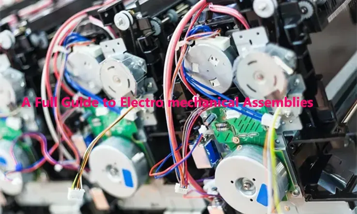
JarnisTech is a distinguished provider of electromechanical assemblies, which are essential components in electrical and electronic systems utilized across various industries, including aerospace, communications, military, and power generation. These assemblies combine electrical circuitry with mechanical parts, and their design and construction must be approached with great care to ensure optimum functionality and manufacturability. Electromechanical assemblies can range from simple to highly complex, and a thorough understanding of their types and applications is vital. In this guide, our team of experts has compiled comprehensive information on electromechanical assemblies, including their definition, available types, and the industries and applications where they are utilized.
What Is An Electro Mechanical Assembly ?
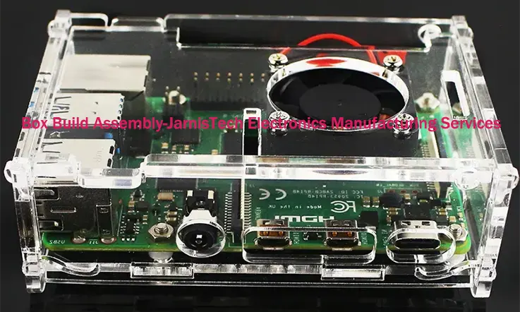
Electro-mechanical assemblies are an amalgamation of electronic and mechanical components housed together in a consolidated package. These assemblies encompass subsystem assemblies that incorporate board-level interconnects and chassis wiring, as well as full system assemblies known as box builds. The range of electro mechanical assemblies is diverse, including box builds, chassis, enclosures, DIN rail assembly, LED assembly, fan trays, switch assembly, fan modification, power panel assemblies, and fan assembly.
There are also specific mechanical assembly products, such as displays, barcode readers, blowers, fans, and terminal blocks, which can be integrated into electro mechanical assemblies for enhanced functionality.
Electro mechanical assemblies are extensively utilized in various industries and applications, including medical, clean technology, industrial, computers, homeland security, communications, marine, test and instrumentation, and satellite communications. The diversity of these applications illustrates the significance of electro mechanical assemblies in modern technology and highlights the need for their reliable design and manufacturing to ensure optimal performance.
Types of Electromechanical Assemblies
Electromechanical assemblies are specifically designed and constructed to perform a particular function. Some of the most commonly manufactured electromechanical assemblies include:
Cable and Harness Assemblies: Cables and harness assemblies comprise cables or wires that transmit electrical power or signals.
Transformer Assemblies: Transformers transfer electrical energy between two or more electrical circuits. They increase or decrease the voltage level according to the requirements of the application.
Power Supply Assemblies: Power supplies provide electrical power to at least one electric load by converting a current to the correct format and voltage required to power it. Power supplies can be designed as standalone devices or incorporated into appliances.
DIN Rail Assemblies: DIN rails, also known as mounting rails, are used to mount other components within an electromechanical assembly. They must be configured according to the components and subassemblies.
Panel Assemblies: Some electromechanical assemblies are integrated into panels, which serve as a means of controlling the distribution of electrical power into connected circuits.
Switch and Sensor Assemblies: Two vital components of electronic systems are switch assemblies and sensor assemblies. Switch assemblies typically connect or disconnect a power supply to electrical components, while sensor assemblies convert stimuli, such as sound, heat, light, or motion, into electrical signals.
Components used in Electro Mechanical Assemblies
Electromechanical assemblies are devices that combine electrical and mechanical components to perform a specific function. There are many different types of electromechanical assemblies, including:
Relays: These are simple electromechanical devices that use an electromagnetic coil to switch a set of contacts on or off. Relays are commonly used in applications such as control systems, safety devices, and power distribution.
Solenoids: Solenoids are electromechanical devices that use a magnetic field to move a plunger or valve. They are often used in automotive, industrial, and medical applications.
Actuators: Actuators are devices that convert electrical energy into mechanical motion. They can be used to move valves, switches, or other mechanical components.
Motors: Motors are devices that convert electrical energy into rotational motion. They are used in a wide range of applications, including manufacturing equipment, robotics, and transportation.
Sensors: Sensors are devices that detect changes in their environment and convert them into electrical signals. They can be used to measure temperature, pressure, position, and many other variables.
Generators: Generators are devices that convert mechanical energy into electrical energy. They are used in power generation, renewable energy systems, and backup power systems.
Transformers: Transformers are devices that transfer electrical energy from one circuit to another using magnetic induction. They are used to step up or step down voltage levels in power distribution systems.
Actuated valves: Actuated valves are valves that are operated by an actuator, which can be electric, pneumatic, or hydraulic. They are used in a wide range of industrial applications, including chemical processing, oil and gas, and water treatment.
These are just a few examples of the many types of electromechanical assemblies that are used in various industries.
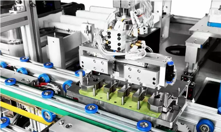
Assembly Process of Electro Mechanical Assemblies
The assembly process of Electro Mechanical Assemblies involves several steps, including planning and preparation, component placement and fastening, wiring and soldering, and testing and quality control. Here is a more detailed breakdown of each step:
1. Planning and Preparation: This step involves reviewing the design specifications and determining the required components and tools. The assembly technician will also plan the assembly sequence and make sure all necessary materials and tools are available.
2. Component Placement and Fastening: In this step, the assembly technician places the components in their designated locations and fastens them using screws, bolts, or other fasteners. It is important to ensure that all components are properly aligned and secured to prevent any potential issues during operation.
3. Wiring and Soldering: Once the components are in place, the wiring and soldering process begins. The assembly technician will connect the electrical and electronic components as per the design specifications, and solder them in place using a soldering iron. It is crucial to ensure that all connections are properly made and that there are no loose wires or cold solder joints.
4. Testing and Quality Control: Once the assembly is complete, it undergoes testing and quality control to ensure that it meets the required specifications. The assembly technician may use various testing equipment such as multimeters, oscilloscopes, and function generators to verify the assembly’s performance. Any issues are identified and corrected, and the assembly is retested until it meets the required specifications.
Overall, the assembly process of Electro Mechanical Assemblies requires precision, attention to detail, and careful testing to ensure that the final product meets the required specifications and performs as expected.
Electro Mechanical Assembly By Outsourcing
Electromechanical assembly work is a complex process that involves assembling various electrical and mechanical devices that interact with each other and respond to received signals. These devices include control panels, controllers, sensors, compressors, and more. Assembling such complex systems requires expertise in design, assembly, and operation of electro mechanical products.
If your company lacks the necessary expertise, outsourcing the electro mechanical assembly work to a specialized contractor like JarnisTech is an excellent choice. By doing so, you can fill the expertise gap in your company and focus on other aspects of your business.
At JarnisTech, we possess extensive knowledge of various electrical and mechanical devices, and we have provided electro mechanical assembly services to customers across a wide range of industries. Our team of engineers collaborates with you throughout the project to deliver a custom-tailored solution, no matter how complex the assembly work may be. We ensure that you receive a high-quality electro mechanical assembly service that meets your requirements precisely.
Our Capabilities in Electro Mechanical Assembly
JarnisTech is a leading provider of electromechanical assemblies, with expertise in handling a wide range of assemblies, including PCB assemblies (BGA, uBGA, CSP), cable assemblies, and box build assemblies. Our team specializes in various electromechanical assembly techniques, such as Surface Mount Technology, Through-hole Technology, Additive Manufacturing, Complex RF Electro-Mechanical, and more.
Our state-of-the-art in-house CNC machining capabilities enable us to manufacture parts with different geometric shapes using advanced 3-axis, 4-axis, and 5-axis milling machines. This gives us the flexibility to provide customized solutions to meet the specific needs of our clients.
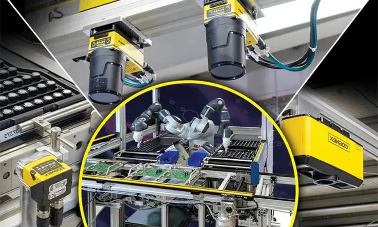
At JarnisTech, we never compromise on quality and perform stringent inspection and testing processes to ensure that our products meet the highest standards. Our testing and inspection processes include Solder Paste Inspection, Automated Optical Inspection (AOI), X-ray Inspection, Visual Inspection, In-circuit Testing, Functional Testing, and more.
Our commitment to quality and expertise in electromechanical assembly techniques make us a reliable partner for any project. We work closely with our clients to provide tailored solutions that meet their unique requirements, resulting in high-quality products that exceed their expectations.
Why Choose Us ?
Our commitment to quality assurance is reflected in our adherence to the highest quality standards. Our certificates, including ISO9001, ISO 13485, IPC, and UL, serve as a testament to the exceptional quality of our assemblies.
We pride ourselves on our high level of flexibility, which enables us to deliver customized assembly services tailored to meet the unique needs of each customer. Our flexibility allows us to handle various electromechanical assembly needs, from simple to complex.
Our strong network of suppliers enables us to source high-quality components quickly and efficiently, based on the specifications provided by our customers. This helps simplify supply chains and reduces costs for our customers.
At JarnisTech, we understand the importance of on-time delivery and are committed to meeting our customers’ deadlines. Our state-of-the-art facilities and streamlined in-house manufacturing processes allow us to deliver electro mechanical assemblies to our customers on time, every time.
Importance of Testing and Inspection in Electro-Mechanical Assemblies
Testing and inspection are crucial steps in the electro-mechanical assembly process. They ensure that the final product meets the required specifications and quality standards, and they help to identify and eliminate defects and failures that can lead to costly rework, recalls, or even safety hazards. Here are some specific reasons why testing and inspection are important in electro-mechanical assemblies:
Verification of Functionality: Testing ensures that the electro-mechanical assembly performs its intended function correctly. It verifies that all components are connected and functioning as expected, and it detects any malfunctions or errors that may occur during operation.
Detection of Defects and Failures: Inspection helps to detect defects and failures that may occur in the electro-mechanical assembly. These defects may be due to manufacturing defects, design flaws, or environmental factors. By identifying these defects early on, they can be corrected before the assembly is shipped or installed.
Compliance with Standards and Regulations:Testing and inspection help to ensure that the electro-mechanical assembly meets the relevant industry standards and regulations. These standards may include requirements for safety, performance, reliability, and environmental impact.
Quality Assurance: Testing and inspection are essential for maintaining the quality of the electro-mechanical assembly. They help to identify and correct any deviations from the expected quality level, and they provide a way to monitor and improve the quality of the assembly over time.
Cost Savings: Testing and inspection can save money by reducing the need for rework, recalls, and warranty claims. By identifying and correcting defects early on, they can prevent costly delays and repairs, and they can improve the overall efficiency and effectiveness of the assembly process.
Therefore, testing and inspection are critical steps in ensuring that electro-mechanical assemblies meet the required standards and specifications, and they help to prevent defects and failures that can lead to costly rework, recalls, or safety hazards.
Industrial Applications of Electromechanical Assemblies
Electromechanical assemblies are used in a wide range of industrial applications due to their ability to combine electrical and mechanical components to perform specific functions. Some of the most common industrial applications of electromechanical assemblies include:
Manufacturing
Electromechanical assemblies are used in manufacturing equipment such as conveyors, robots, and assembly lines. They can be used to move parts, control processes, and ensure quality control.
Automotive
Electromechanical assemblies are used in automotive applications such as actuators for power windows and locks, sensors for airbags and anti-lock brakes, and motors for windshield wipers and power seats.
Aerospace
Electromechanical assemblies are used in aerospace applications such as actuators for landing gear and flight control surfaces, sensors for navigation and control, and motors for pumps and generators.
Energy and Power
Electromechanical assemblies are used in energy and power applications such as generators, transformers, and motors for power generation, distribution, and conversion.
Medical
Electromechanical assemblies are used in medical applications such as actuators for surgical instruments, sensors for patient monitoring, and motors for medical equipment such as pumps and ventilators.
Robotics
Electromechanical assemblies are used in robotics applications such as actuators for robot arms and grippers, sensors for navigation and control, and motors for movement and power.
Packaging
Electromechanical assemblies are used in packaging applications such as conveyors, sensors for product detection and tracking, and actuators for packaging equipment such as filling machines and labelers.
Agriculture
Electromechanical assemblies are used in agriculture applications such as actuators for irrigation systems, sensors for monitoring soil moisture and temperature, and motors for equipment such as tractors and harvesters.
These are just a few examples of the many industrial applications of electromechanical assemblies. They are widely used in many different industries due to their versatility and ability to meet specific application requirements.
Future of Electro Mechanical Assembly
The future of Electro Mechanical Assembly looks promising with the advancements in technology and the increasing demand for automation and robotics. Here are some potential developments that could shape the future of Electro Mechanical Assembly:
Miniaturization: With the increasing demand for smaller, lighter, and more efficient devices, Electro Mechanical Assemblies will continue to be miniaturized. This will require the development of new, smaller components and assembly techniques.
Automation: Automation in Electro Mechanical Assembly will increase, with the use of robotics and other automated systems to perform tasks such as component placement, soldering, and testing. This will lead to faster, more efficient assembly processes and higher productivity.
Additive Manufacturing: Additive manufacturing (3D printing) is already being used in some Electro Mechanical Assemblies, and this trend is expected to continue. 3D printing will enable the production of complex geometries and customized parts, reducing the need for assembly of multiple components.
Integration with Electronics: There will be an increased integration of Electro Mechanical Assemblies with electronics, as the lines between mechanical and electronic components continue to blur. This will require new skills and knowledge for assembly technicians.
Sustainable Manufacturing: There will be a growing focus on sustainable manufacturing in Electro Mechanical Assembly, with a shift towards the use of environmentally friendly materials and processes. This will require the development of new, sustainable assembly techniques and materials.
Conclusion
Electro Mechanical Assembly is a critical process in the manufacturing of a wide range of products, from simple switches to complex control systems. It involves the assembly of mechanical, electrical, and electronic components to create functional systems that meet specific requirements.
The types of Electro Mechanical Assemblies can vary from basic to complex, depending on the application and required functionality. As technology advances, the future of Electro Mechanical Assembly looks promising, with developments such as miniaturization, automation, additive manufacturing, integration with electronics, and sustainable manufacturing expected to shape the industry.
Overall, Electro Mechanical Assembly plays a crucial role in modern manufacturing, and its continued evolution and innovation will enable the creation of new and exciting products that meet the needs of an ever-changing world.
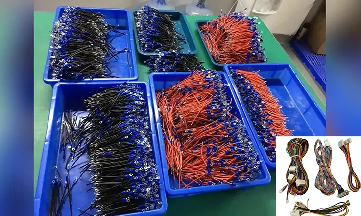
With an extensive track record spanning two decades, JarnisTech stands out as a trusted provider of premium custom cable and harness assemblies to global high-tech clientele. Our repertoire includes a diverse set of processes like manufacturing, ultrasonic welding, and injection molding, enabling us to deliver exceptional products and services across a broad spectrum of complexity, ranging from simple to intricate cable and harness assemblies. Whether clients require prototypes or turnkey solutions, we consistently meet their diverse needs with precision.
At JarnisTech, we understand the value of efficient and real-time communication. That’s why our exceptional team is adept at facilitating seamless collaboration, expediting the assembly process and ensuring speedy time-to-market results.
Our wire harness assemblies can be tailored to possess a versatile range of properties and conform to various industry standards. Beyond ensuring continuity and functionality through comprehensive testing, we also offer specialized services such as box assembly and cleanroom assembly (Class 10,000). Quality is of utmost importance to us, which is why our facilities hold ISO 9001:2008 certification. Through stringent testing and robust quality control measures, we ensure that all our products consistently adhere to the same exceptional standards.
To gain deeper insights into our comprehensive custom cable and harness assembly services, we encourage you to reach out to us directly.
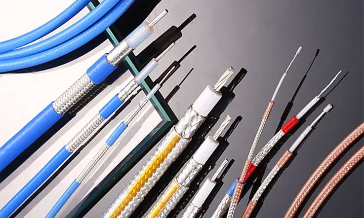
Wire Harness Assembly(Sometimes called a cable) Definition
The primary function of a wire harness assembly is to address challenges related to electrical requirements and spatial limitations within electrical systems. It serves to provide physical support and organization for a collection of cables and wires within a designated space. While wire harnesses are primarily used for organizational purposes in applications with less demanding requirements, they are not typically suitable for outdoor use or in environments with potential environmental hazards.
Referred to as cable or wiring looms, harness assemblies effectively arrange groups of wires and/or cables into a unified unit for protection and organization. They incorporate a variety of terminals and connectors that are strategically positioned and routed to the various connection points of an assembly. Wire harnesses offer an economical electrical solution specifically designed to streamline wiring systems.
Maintaining precise lengths and orientations of wires and cables is paramount to ensure efficient and straightforward installation processes. Assemblies can encompass a diverse range of cable or wire constructions, sizes, colors, and materials, all selected according to the specific application requirements.
A typical harness assembly utilizes sleeved wires and/or multi-conductor cables held together by ty wraps or tubing, which both safeguard and organize the bundled wires and cables. Unique terminations, such as plug or socket arrangements, are often necessary for specific applications, and are appropriately attached to the wires. Given the multitude of potential variables involved, all wire harnesses are customized to suit their intended operating environment.
Wire Harness Fabrication
The wires required for the harness are initially trimmed to the desired length and appropriately labeled. Subsequently, the wire ends are stripped to expose the uninsulated conductor and equipped with necessary terminals or connector housings. The wires and components are thereafter assembled on the pin-board according to the desired specifications, and finally secured together.
Why Are Wire Harnesses Assembled Manually?
The wire harness assembly process remains predominantly a manual operation, as it encompasses a range of intricate procedures that are more effectively carried out by human hands rather than automation. These manual processes involve:
● Installing terminated wires of varying lengths.
● Routing wires and cables through sleeves and conduits.
● Applying tape to secure wire breakouts.
● Executing multiple crimps.
● Binding components together using tape, clamps, or cable ties.
Due to the complexity of automating these tasks, manual production continues to be the more cost-efficient option, particularly when dealing with small production runs. Consequently, harness production generally requires a longer timeframe compared to other types of cable assemblies, ranging from a few days to several weeks. The level of intricacy in the design directly influences the duration of the production process.
Nevertheless, there are specific pre-production stages that can benefit from automation, such as:
● Employing automated machines to cut and strip wire ends individually.
● Utilizing automated crimping systems to attach terminals on one or both sides of the wire.
● Inserting wires, pre-fitted with terminals, into connector housings.
● Employing automated soldering processes for wire end connections.
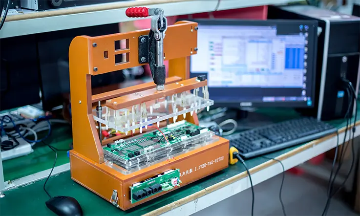
Following the completion of the wire harness assembly process, the crucial final step involves testing the harness for its electrical functionality. To accomplish this, a specially designed and pre-programmed test board is utilized. The test board is configured with the necessary electrical specifications, and the fully assembled harness is connected to the board for a comprehensive fault-checking procedure.
We hope that this article has provided comprehensive insights into wire harness assemblies and addressed most of your inquiries. If you are considering the implementation of a custom wire harness solution and require further clarification, we are here to assist you with the information you require.
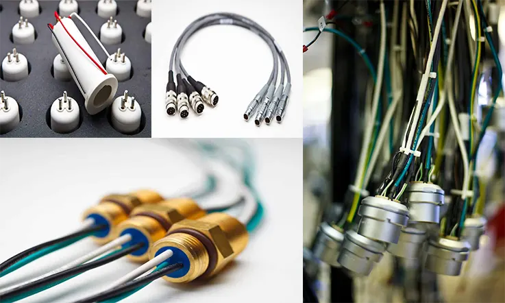
Wire Harness vs. Cable Assembly
Cable assembly and wire harness are occasionally mistaken for being identical, owing to their overlapping functionality. This confusion is understandable since professionals often interchangeably use these products, which serve similar basic functions. However, it is important to note that cable assemblies and wire harnesses are distinct from one another.
Though harnesses and assemblies seemingly serve the same purpose (analogous to wires and cables), their differentiation lies in their capabilities.
Wire Harnesses
Wire harnesses consist of a collection of individually sheathed wires that are grouped together to create a cohesive unit. This assemblage of wires serves the purpose of providing electrical connectivity while ensuring the organization of electrical components. Wire harnesses are particularly advantageous in situations where space is limited, although they also find applications in large-scale systems. One key benefit of utilizing wire harnesses is their ease of installation. Instead of individually routing multiple single wires throughout a system, harnesses consolidate the wires, allowing for simultaneous routing to streamline the process and mitigate the occurrence of human errors.
Cable Assemblies
A cable assembly refers to the consolidation of multiple cables or wires that are intricately braided and enveloped within a single safeguarding sheath, resulting in a unified assembly. Similar to wire harnesses, cable assemblies offer electrical connectivity while effectively organizing wires and cables. However, their primary purpose is to afford protection to the internal wires and cables against various mechanical and environmental elements.
The exterior appearance of a cable assembly exhibits a straightforward design, featuring a robust thermoplastic material. This outer layer serves as a shield, guarding the internal components from application-specific demands, such as extreme temperatures, friction, vibrations, weather conditions, chemical exposure, UV radiation, strain, and other environmental and mechanical factors.
To ensure the suitability of a cable assembly for the intended application environment, most manufacturers provide a range of readily available solutions, as well as considerable flexibility for customization and design. While this may entail initial investment costs, the return on investment is swiftly realized through enhanced performance, heightened reliability, and prolonged lifespan of the cable assembly solution.
Cable & Wire Harness Assembly Benefits
In various industries, the organization of wires and cables connected to electrical devices is of utmost importance, and wire harnesses and cable assemblies play a critical role in achieving this organization effectively.
Many Prominent wire harness manufacturers can offer custom-made wire and cable harness assemblies based on customer specifications, resulting in saved time and improved organization.
Wire and cable harness assemblies deliver numerous benefits, including:
Reduced installation time: Vehicles, for example, often require extensive wiring. Wire harness assemblies simplify the manufacturing process by integrating all the necessary wires and cables into a single unit. Installation then becomes a straightforward task of incorporating the harness, eliminating the need for individual wire routing.
Enhanced security and safety: Binding wires and cables within a harness increases the overall stability and protection against vibrations, abrasions, and moisture. Optimal space utilization and the absence of flexing in a bundled configuration reduce the risk of electrical shorts. Moreover, using flame-retardant sleeves further diminishes the likelihood of electrical fires.
Lower cable installation costs: The use of cable harnesses and assemblies can improve cable installation efficiency, resulting in cost savings.
Improved system performance & reliability: Implementing cable assemblies and wire harnesses enhances system performance and reliability. They offer superior protection to wires against harsh external factors commonly encountered in various environments.
Weight and space savings: Cable harnesses and assemblies contribute to reduced weight and space requirements by facilitating cable organization and consolidation.
Enhanced safety: Wire and cable harness assemblies eliminate the risk of tangled and exposed wires, thereby improving overall safety. Inspection procedures are also simplified through the utilization of organized harness configurations.
By leveraging wire harnesses and cable assemblies, industries can benefit from improved productivity, cost-efficiency, system performance, and safety in their electrical installations.
With over two decades of experience serving global high-tech customers, JarnisTech is a trusted provider of premium custom cable and harness assemblies. Our commitment to delivering the highest quality products sets us apart.
At JarnisTech, we offer discrete cable and harness assemblies for various cable types, including flat ribbon cables, RF cables, fiber optic cables, and multi-conductor cables. Our extensive range of processes, such as manufacturing, ultrasonic welding, and injection molding, ensures that we deliver exceptional products and services.
As a turnkey solution provider, JarnisTech caters to mid-scale prototypes, offering a comprehensive cable and harness assembly service. Our focus on fast delivery, efficient component sourcing, precise assembly, and 100% continuity testing ensures that our customers receive top-notch solutions.
Our dedicated team is equipped to provide real-time and efficient communication, ensuring smooth execution and handling of any engineering change orders (ECOs) that may arise during the cable assembly process. We prioritize effective collaboration and clear communication channels to guarantee customer satisfaction.
Why Choose Us ?
Design and Engineering: At JarnisTech, we leverage AutoCAD to develop product concepts and create assembly layouts, allowing us to envision and refine designs effectively. Additionally, we offer prototype development services to address any unforeseen challenges that may arise during the design phase, ensuring optimal solutions.
Component Sourcing: With an extensive supplier network, JarnisTech excels in sourcing high-quality components at competitive prices. Our streamlined procurement process and strong relationships with trusted suppliers enable us to obtain the best components for your project.
Cable & Wire Harness Assembly: Equipped with advanced technology and a team of highly skilled engineers and production staff, we specialize in the assembly of diverse cable and wire harness configurations. From straightforward to intricate designs, we have the expertise and capabilities to deliver exceptional results.
Testing and Inspection: Quality is paramount at JarnisTech, which is why we provide reliable testing services to ensure the functionality and reliability of our cable and wire harness assemblies. Our testing capabilities include comprehensive assessments such as 100% continuity testing, break testing, custom harness fixtures for production testing, resistance testing for multiple harness combinations, and withstand voltage testing.
Future Trends and Innovations in Cable and Wire Harness Assembly
Future trends and innovations in cable and wire harness assembly are driven by advancements in technology and evolving industry demands. Here are some notable trends to keep an eye on:
High-Speed and Fiber Optic Wiring: With the increasing need for high-speed data transmission, there is a shift towards using fiber optic cables and high-frequency wiring in cable and wire harnesses. These technologies offer greater bandwidth, signal integrity, and immunity to electromagnetic interference.
Smart Harnesses and Integrated Electronics: The integration of electronics directly into cable and wire harnesses enables additional functionalities and intelligence. Smart harnesses may include sensors, microcontrollers, and communication interfaces to monitor and control various parameters, enhancing efficiency and diagnostics.
Industry 4.0 and Automation: The adoption of Industry 4.0 principles, such as digitalization, automation, and connectivity, is revolutionizing cable and wire harness assembly. Automation technologies like robotic assembly, computer-aided design, and augmented reality-based instructions are improving production efficiency and quality control.
Advanced Testing and Quality Assurance: Quality control and testing of cable and wire harnesses are becoming more sophisticated. Advanced testing methods, such as automated testing systems, in-line inspection, and functional testing, ensure the reliability and performance of the assembled products.
Wirelessly Powered and Connected Harnesses: Wireless power transfer and wireless communication technologies are being explored to eliminate physical wires in certain applications. These wireless harnesses can transmit power and data without the need for conventional cables, reducing weight and complexity.
Predictive Maintenance and Condition Monitoring: The integration of sensors and data analytics in cable and wire harnesses allows for predictive maintenance and condition monitoring. Real-time monitoring of parameters like temperature, vibration, and current draw can help identify potential failures before they occur, enhancing reliability and reducing downtime.
These are just a few trends shaping the future of cable and wire harness assembly. As technology continues to advance, we can expect further innovation and advancements in this field.
Summary
The future of cable and wire harness assembly is driven by technological advancements, evolving industry needs, and the pursuit of enhanced performance, reliability, and efficiency. As these trends continue to develop, we can expect further innovations in the field, enabling the creation of more advanced and sophisticated electrical systems in various applications.
At JarnisTech, we take great pride in our exceptional ability to manufacture high-quality electronic components with a near-zero attrition rate. Our IC products boast an attrition rate of 0%, while our Capacitor and Resistor components have a rate of just 0.3%. Our precision assembly techniques enable us to produce incredibly accurate chips, including 03015 chip/0.35 pitch BGA.
We understand that the key to providing our customers with the lowest possible manufacturing costs lies in the procurement of low-cost components. To achieve this, we have a dedicated sourcing team that utilizes reliable channels to obtain components at the lowest prices available in the global market, even for those that are typically hard to find.
Our extensive range of products includes active component assemblies such as IC integrated circuits, memory chips, diodes, transistors, as well as passive components like capacitors, resistors, inductors, and electromechanical components such as connectors and switching devices. We also specialize in sourcing other hard-to-find special electronic components.
At JarnisTech, we are committed to providing our customers with the highest quality products at the most competitive prices. We achieve this by utilizing our expertise in precision assembly techniques and reliable sourcing channels to deliver exceptional electronic components that meet the needs of a wide range of industries and applications.
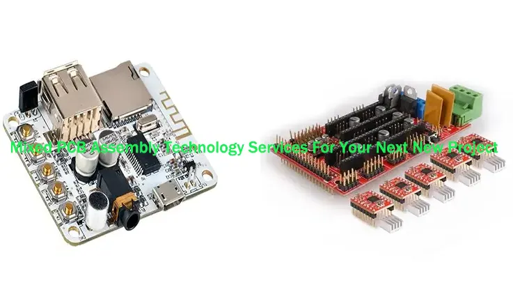
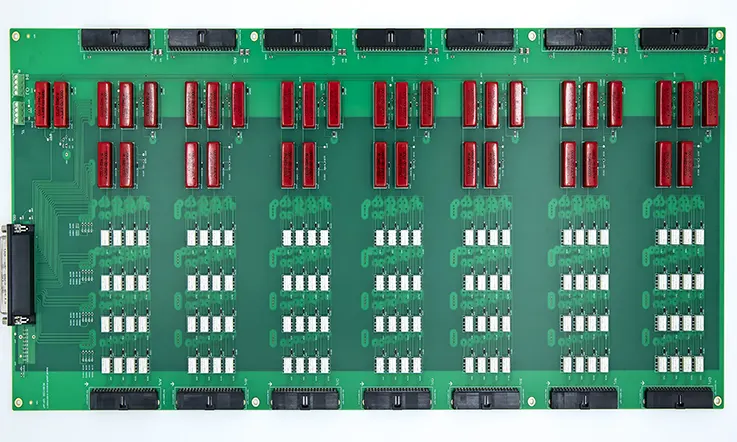
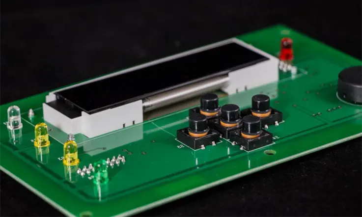
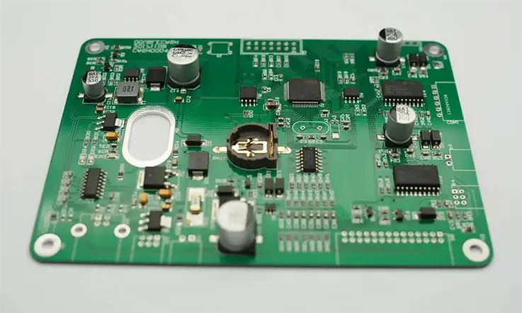
Electronics Assembly Components
In the realm of electronics, a printed circuit board (PCB) can be likened to a living organism with each component serving as a vital organ. The copper traces of the PCB can be considered the skeleton, providing essential structural support. Each electronic component plays a unique role in imparting the circuit with the specific qualities necessary to perform its intended function. Depending on the type of electronic equipment or device for which the bare PCB circuit board is designed, a range of diverse components may be required for various circuits.
Some of the most commonly used electronic components in PCB assembly include:
Battery – an indispensable component that acts as the voltage or current source for the circuit. Without it, the PCB cannot function unless directly connected to a DC source.
Resistors – a form of amplifier used to switch or control the electronic signals within the board. While transistors come in various types, the most common is the bipolar transistor, which has three pins: the collector, base, and emitter.
Inductors – similar in nature to capacitors, these components store energy as a magnetic field when current flows through them. Inductors are primarily used to block unwanted signals in a PCB board, such as interference from other electronic devices or equipment.
Capacitors – second in popularity only to resistors, capacitors hold an electrical charge in the circuit board and release it when extra power is needed elsewhere. This is achieved by the two conductive layers of the capacitor holding opposite charges, separated by an insulating material.
Diodes – miniature devices within a circuit responsible for allowing the unidirectional flow of electrical current. Diodes are used to stop or block current flow in an unwanted direction and can include popular examples such as LEDs used for emitting light.
Transformers – essential components used to transfer electrical energy from one circuit to another by increasing or decreasing the voltage.
Sensors – critical electronic components that detect environmental changes and generate corresponding electrical signals. These signals are then sent to other circuit components. Sensors convert physical elements such as air quality, light, motion, or sound into electrical energy.
At the heart of any PCB is the careful selection and integration of high-quality electronic components. These components work together to create a functional and reliable circuit board that meets the specific needs of the intended application.
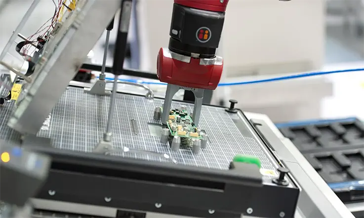
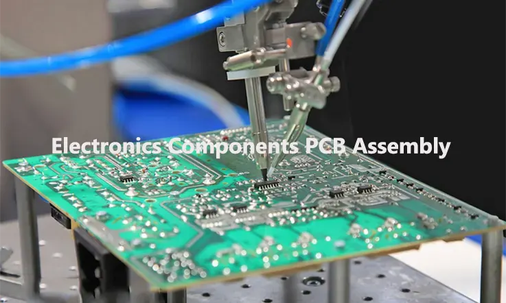
How Does PCB Electronics Components Assembly Work?
PCB assembly (PCBA) is a process of assembling electronic components onto a printed circuit board (PCB) to create a functional electronic device. The following are the steps involved in PCBA components assembly:
1. Solder Paste Application: Solder paste is applied to the PCB using a stencil. The stencil ensures that the solder paste is applied only to the correct locations on the PCB.
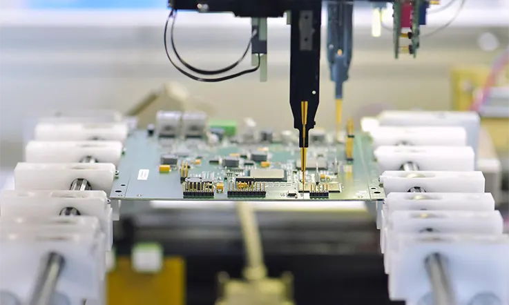
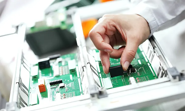
2. Component Placement: The components are placed onto the PCB using automated equipment. This is done by using pick-and-place machines that take the components from their reels and place them onto the PCB.
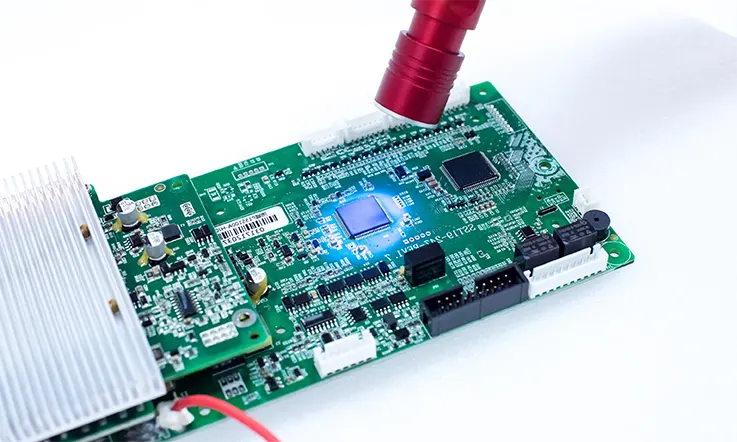
3. Reflow Soldering: Once the components are placed onto the PCB, the board is heated in a reflow oven. The oven melts the solder paste, which then creates a permanent bond between the components and the PCB.
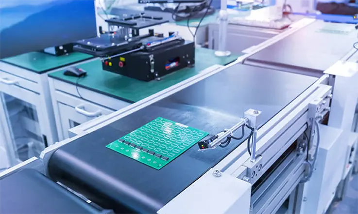
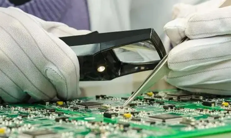
4. Inspection: After the reflow soldering process, the PCB is inspected to ensure that all components are properly placed and soldered. The inspection can be done manually or using automated inspection equipment.
5. Testing: Once the inspection is complete, the PCB is tested to ensure that it functions as intended. Various tests such as functional testing, in-circuit testing, and boundary scan testing are performed to check the functionality of the PCB.
6. Final Assembly: Once the PCB has passed all the tests, it is assembled into the final product. This can involve adding additional components, enclosures, and packaging.
Overall, PCBA components assembly is a complex process that requires specialized equipment and expertise. It is an essential step in the manufacturing of electronic devices.
Type of Electronic PCB Assembly
There are several different types of electronic PCB assembly, including:
Through-Hole Assembly
This is the traditional method of PCB assembly, where components are inserted into pre-drilled holes on the PCB and then soldered onto the board.
Surface Mount Technology (SMT) Assembly
This method involves mounting components directly onto the surface of the PCB without the need for pre-drilled holes. SMT components are much smaller and can be placed closer together, allowing for more compact designs.
Mixed Technology Assembly
This involves using both through-hole and SMT components on the same PCB. This method is often used when a PCB requires both large components that need to be through-hole mounted and small components that need to be SMT mounted.
Ball Grid Array (BGA) Assembly
This method is used for mounting components that have a large number of pins, such as microprocessors and memory chips. BGA components have a grid of small solder balls on the underside that are used to make contact with the PCB.
Package-on-Package (PoP) Assembly
This method involves stacking one or more components on top of another component, allowing for more components to be mounted in a smaller space.
Chip-on-Board (CoB) Assembly
This method involves mounting bare semiconductor chips directly onto the PCB. This method is often used in applications where size and weight are critical factors.
Each of these assembly methods has its advantages and disadvantages, and the most appropriate method will depend on the specific requirements of the PCB and the final product.
How to Find the Right Electronics Component PCBAssembly Maker?
Finding the right electronics component PCB assembly maker can be a daunting task, but there are a few steps you can take to ensure that you choose the right company for your needs. Here are some suggestions:
Look for experience and expertise
Check the company’s website and look for information about their experience in the industry, their areas of expertise, and the types of projects they have worked on. A company with experience and expertise will be able to provide you with high-quality PCB assembly services.
Check the company’s certifications
Look for companies that have certifications such as ISO 9001:2015, IPC-A-610, and J-STD-001. These certifications indicate that the company follows industry standards and best practices.
Consider the company’s equipment and technology
Check the company’s equipment and technology to ensure that they are up-to-date and can handle your project’s requirements. A company with advanced equipment and technology will be able to provide you with high-quality PCB assembly services.
Check the company’s customer service
Communication is crucial in the PCB assembly process, so it’s important to choose a company with excellent customer service. Look for a company that is responsive, communicative, and willing to work with you to meet your needs.
Ask for references and reviews
Don’t be afraid to ask the company for references or reviews from previous customers. This can help you gauge their reputation and the quality of their work.
Compare quotes
Finally, get quotes from multiple companies and compare their prices, services, and capabilities. This will help you choose the best option for your project’s needs and budget.
By following these steps, you can find the right electronics component PCB assembly maker for your project.
Why Choose Us?
Advantages of JarnisTech in electronics Components PCB Assembly:
Our supply chain guarantee is one of our key advantages
We work closely with well-known brand manufacturers and agents to ensure that our customers receive only original and new products, free of fake and substandard items. Our professional IQC team conducts strict inspections on every part to guarantee that each product is genuine, and we offer our customers the most competitive prices for PCB and PCB assembly.
We offer a comprehensive range of products, including integrated circuits (ICs), MOS field-effect transistors, diodes, Schottky, voltage regulators, silicon-controlled rectifiers, optical couplers, IGBT/power tube patch LED, capacitors, resistors, inductors, connectors, and more. Our wide channels and international collaborations with leading brands enable us to provide the highest quality products to our customers.
Fast Delivery is Another of Our key Advantages
We have established stable channels and hold a large amount of inventory to ensure rapid delivery of components. Our supply of conventional components is consistent, and we guarantee that there are no order delays.
We practice full supply chain management and purchase only from franchisees or directly from component manufacturers to ensure full traceability. This allows us to obtain the best opportunities and price points while ensuring that all suppliers are trustworthy and reliable, and that the procurement process is fully traceable.
With our many years of distribution and inspection experience, we provide our customers with the most reliable products and services. Our professional team is quick to respond to inquiries and orders, and they have a wealth of experience and understanding of market trends, enabling us to provide cost-effective services to our customers. Customers can provide us with individual product information or a full BOM, and we will provide them with a product quotation and delivery time as soon as possible.
JarnisTech: Quality & Professional Service You Can Trust
At Jarnistech, we understand that quality is crucial in PCB production. That’s why we are committed to ensuring that our customers receive the best possible final quality PCBs. All of our manufacturing facilities are ISO 9001 certified, and we regularly update our equipment to meet our customers’ PCB requirements.
Our dedication to quality has earned us a growing customer base, with over 150 new customers registering with us every day. Many of these customers come to us through referrals from our satisfied customers. Our quality control engineers conduct routine inspections of PCBs during production and before shipment to ensure that they meet our high standards. In addition to visual checks, we use appropriate testing machines to test 100% of the boards.
Quality is the cornerstone of our business, and we understand that the PCB business requires the involvement of professional engineers to clarify technical specifications and troubleshoot technical problems with our customers. Our engineers are trained professionals who provide a free engineering file review service to check your orders before transferring them to fabrication sections to minimize errors.
Our engineers are also skilled businessmen who know how to save costs for our customers while maintaining high-quality standards. We guarantee that all shipped PCBs are compliant with your requests, and we conduct a thorough quality check before shipment to ensure that our customers receive the best possible product.
At Jarnistech, we are committed to providing our customers with the highest quality PCBs and exceptional customer service. We believe that our dedication to quality is the main factor in our growing reputation and word-of-mouth referrals, which help us to expand our business globally.
Common Issues in Electronics Components and PCB Assembly
There are several common issues that can occur in electronics components and PCB assembly. These issues can affect the performance and reliability of the system or device, and may require troubleshooting and repair to resolve. Here are some examples:
Component Issues: Faulty or damaged components can cause a range of problems, such as incorrect operation, intermittent faults, or complete failure. This can be caused by manufacturing defects, damage during shipping or handling, or issues with the component’s design or specifications.
Soldering Issues: Poor soldering can cause issues such as cold joints, solder bridges, or insufficient solder. This can result in intermittent faults, poor connectivity, or complete failure. Soldering issues can be caused by incorrect soldering techniques, poor quality solder, or issues with the PCB design or layout.
PCB Layout Issues:PCB layout can have a significant impact on the performance and reliability of a system or device. Poor layout can cause issues such as noise, crosstalk, or signal integrity problems. This can be caused by issues with the design or layout software, incorrect component placement, or poor routing.
Environmental Issues: Environmental factors such as temperature, humidity, and vibration can affect the performance and reliability of electronics components and PCBs. This can cause issues such as corrosion, thermal stress, or mechanical failure.
Power Supply Issues: Power supply issues such as overvoltage, undervoltage, or noise can cause a range of problems in electronics components and PCBs. This can affect the operation of the system or device, and may cause damage to components or the PCB itself.
Firmware and Software Issues: Issues with firmware or software can cause a range of problems, such as incorrect operation, crashes, or system failures. This can be caused by bugs in the software, incorrect configuration, or issues with the hardware or firmware.
In summary, common issues in electronics components and PCB assembly can include component issues, soldering issues, PCB layout issues, environmental issues, power supply issues, and firmware and software issues. Identifying and resolving these issues can require a combination of technical knowledge, analytical skills, and experience, as well as the ability to think creatively and outside the box to find solutions to complex problems.
Repair Techniques for Component Assemblies
Repair techniques for component assemblies can vary depending on the nature of the issue and the specific components involved, but here are some common techniques that may be used:
Component Replacement: If a faulty component is identified, it may need to be replaced. This can involve removing the faulty component and installing a new one in its place. Component replacement may require special tools and techniques, such as desoldering tools, heat guns, or specialized pliers.
Soldering and Desoldering Techniques: Soldering and desoldering techniques are used to remove and replace components and to make repairs to solder joints. These techniques can include using a soldering iron, a hot air gun, or a reflow oven. Proper soldering and desoldering techniques are critical to ensure a reliable repair.
PCB Repair and Modification: PCB repair and modification can involve repairing damaged traces or pads, adding or removing components, or modifying the layout of the PCB to improve performance or correct issues. PCB repair and modification may require specialized tools and techniques, such as conductive paint, epoxy, or a PCB milling machine.
Firmware and Software Updates: In some cases, issues with component assemblies may be caused by bugs or issues with the firmware or software. Updating the firmware or software can sometimes resolve these issues. This may involve downloading and installing updates from the manufacturer’s website or using specialized software tools to flash the firmware.
Repair Tips and Tricks: Depending on the specific issue and the components involved, there may be some specialized repair techniques or tricks that can be used to resolve the issue. These can include using specialized tools or equipment, adjusting settings or parameters, or making modifications to the system or device to improve performance or correct issues.
All in all, repair techniques for component assemblies can include component replacement, soldering and desoldering techniques, PCB repair and modification, firmware and software updates, and specialized repair tips and tricks. Proper repair techniques are critical to ensure a reliable repair and to prevent further issues from occurring.
Final Thoughts
PCB components assembly is a critical process in the production of electronic devices. It involves the mounting of various electronic components onto a printed circuit board using automated equipment and then soldering them into place. The components used in PCB assembly can include passive and active devices, as well as connectors and switches.
The assembly process can involve surface mount technology, through-hole assembly, or a combination of both. Testing and inspection are also important steps in the process to ensure that the assembled board is functional and reliable. As technology advances, the future of PCB assembly is likely to involve even more automation and precision, further improving the quality and efficiency of electronic device production.
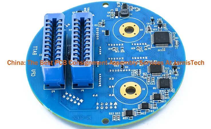
Consignment PCB assembly is a popular solution for businesses seeking to outsource their printed circuit board assembly needs. This approach involves clients sourcing and procuring all the necessary components and then providing them to the assembly company for the final assembly process. This allows clients to have greater control over the manufacturing process and enhances their understanding of the constituent components and the assembly process.
In this article, we will delve deeper into the benefits of consignment PCB assembly, the mounting options available, and how JarnisTech’s services can help businesses streamline their PCB assembly needs.
JarnisTech’s Consignment Assembly Service
In traditional turnkey printed circuit board assembly (PCBA), the manufacturer handles the entire process from sourcing components to assembly and testing. However, consignment PCB assembly is a more adaptable solution in which customers provide all necessary parts and components for assembly.
Consignment PCB assembly offers a mutually beneficial arrangement for both the customer and manufacturer. It provides customers with the flexibility and versatility required for PCB assembly and prototyping, while enabling manufacturers to ensure the fastest turnaround time.
At JarnisTech Electronics, we possess extensive expertise in consignment PCB manufacturing assembly, which empowers our customers to supply the required parts while still maintaining cost-effectiveness. This approach facilitates a rapid product launch for our customers.
Types of Consignment PCB Assembly
There are several types of consignment PCB assembly:
Full Consignment Assembly: In this type of consignment assembly, the customer provides all the required components, including the PCB, electronic components, and any necessary documentation. The assembly company provides the labor and equipment required to assemble the board.
Partial Consignment Assembly: In this type of consignment assembly, the customer provides some of the required components, such as the PCB or the electronic components, while the assembly company provides the remaining components and the assembly labor and equipment.
Kitted Assembly: In kitted assembly, the customer provides all the required components, but in a kit form. The assembly company provides the labor and equipment required to assemble the board.
Each type of consignment PCB assembly has its own advantages and disadvantages, depending on the customer’s requirements and preferences. It is important to choose the right type of consignment assembly to ensure the best quality, efficiency, and cost-effectiveness.
Difference Between Turnkey PCB Assembly and Consigned PCB Assembly
Once you have completed the design phase of your electronics product, the next step is to create a functioning prototype and bring it to market through volume production. To achieve this, you will need to engage the services of a professional who can handle the printed circuit board (PCB) fabrication and assembly. There are two primary approaches available to you at this stage of the project, each with its own cost/benefit and risk/reward considerations.
You can opt to have your electronic manufacturing completed by either a turnkey provider or a consignment provider. It is essential to carefully evaluate each option to ensure that you select the one that best aligns with your needs and business strategy.
Turnkey Assembly
Pros:
The process of manufacturing a printed circuit board (PCB) involves several intricate steps, including circuit board printing and storage, component ordering and warehousing, assembly, and thorough testing to ensure that the final product meets the desired specifications. Transforming a PCB into a successful product requires the installation and shipping of the final product, which can be quite a daunting task.
By leveraging the services of a full turnkey PCB assembly provider, you can outsource all of these complex steps and free up your time to focus on designing innovative products and managing your business operations. This approach allows manufacturing professionals to handle all the aspects outside your area of expertise. With a turnkey manufacturer, you can rely on a single point of contact for any issues or changes that need to be addressed, without the hassle of communicating with multiple vendors to resolve problems.
In addition to simplifying communication, using a turnkey manufacturer can also reduce lead times by eliminating the need for you to procure parts from various suppliers. By sourcing and assembling all necessary components in-house, a turnkey manufacturer can streamline the entire process, resulting in faster production times and a more efficient supply chain.
Cons:
Collaborating with a turnkey manufacturer involves entrusting them with the responsibility of managing the entire production process of your product. Some enterprises may exhibit apprehension towards relinquishing control over their manufacturing operations to an external party. However, selecting a trustworthy manufacturer guarantees that your product will be handled with utmost professionalism. It is essential to thoroughly evaluate various service providers and be self-assured in opting for a turnkey solution.
Consignment Assembly Services
In consignment assembly, the onus is on you to procure and warehouse all the necessary components for your PCB boards. It is imperative to maintain meticulous inventory records to ensure the smooth assembly of your product. Following this, you must pack and dispatch the components to the assembly company. While this approach provides a certain degree of control, it also places a significant burden on your staff to ensure seamless manufacturing operations. It is crucial to evaluate the impact of this approach on the overall manufacture of your product.
Pros:
The extent of control that a company seeks to exert over the manufacturing process after the design phase varies depending on their perspective. Nonetheless, if a reputable turnkey provider with a proven track record of delivering quality work is engaged, it is reasonable to trust that they will ensure that the components meet or exceed the specified requirements and tolerances. However, introducing a third-party manufacturer implies relinquishing control over the entire process. For those who prefer to exercise meticulous control over every aspect of the manufacturing process and have the necessary resources to manage the consignment approach, it is a viable option.
Cons:
Opting for consignment assembly entails assuming a considerable amount of supplementary responsibilities. These include allocating adequate storage space for components, supervising inventory management and procurement of each part, managing multiple supply chains, and sorting, packing, and dispatching the components to the assembly company. This necessitates additional staffing, financial resources, and expertise, which may not be feasible for every business to undertake. Furthermore, any disruption in the supply chain or operational mishaps could potentially arise, necessitating the need for troubleshooting. This means that the consignment approach involves handling several diverse aspects of the process, which requires conscientious problem-solving skills.
How Consignment PCB Assembly Works ?
Consignment PCB assembly is a process where a customer provides all the necessary components and materials to an assembly house, who then assemble and test the printed circuit board (PCB) according to the customer’s specifications. Here are the steps involved in a typical consignment PCB assembly process:
1. Customer provides the assembly house with a bill of materials (BOM) that includes all the necessary components, their quantities, reference designators, and any other specific requirements.
2. The customer also provides the assembly house with the PCB design files, including the Gerber files, pick-and-place files, and assembly drawings. These files are used by the assembly house to program their automated assembly machines and equipment.
3. The assembly house then verifies the BOM and PCB design files to ensure that all the required components and materials are available and match the specified requirements.
4. The customer ships the components and materials to the assembly house, who then inspects and records the received materials.
5. The assembly house then prepares the components for assembly, which may include cutting and forming the leads of through-hole components, taping and reeling the surface-mount components, and programming any required microcontrollers or other chips.
6. The components are then loaded onto the assembly machines, which place them on the PCB according to the pick-and-place files.
7. The assembled PCBs are then sent through a soldering process, which can be done using various methods such as wave soldering, reflow soldering, or hand soldering.
8. Once the soldering process is complete, the assembled PCBs are inspected both visually and with automated equipment to ensure that all the components are properly placed and soldered.
9. The assembled PCBs are then tested to ensure that they meet the customer’s specifications and functions as intended.
10. The completed PCBs are then packaged and shipped back to the customer.
Overall, the consignment PCB assembly process allows customers to have more control over the selection and quality of components used in their PCBs, but also requires them to manage the procurement and logistics of providing those components to the assembly house.
Factors to Consider when Choosing a Consignment PCB Assembly Provider
Choosing the right consignment PCB assembly provider is important to ensure that your PCBs are assembled accurately and efficiently. Here are some factors to consider when selecting a consignment PCB assembly provider:
Experience and Expertise: Look for an assembly house that has a proven track record of successful consignment PCB assembly projects. They should have experienced personnel with expertise in PCB design, assembly, and testing.
Quality Control and Certifications: Check if the assembly house has a quality control system in place and if they are certified to industry standards such as ISO 9001 or IPC-A-610. This ensures that the assembled PCBs meet the required quality standards.
Equipment and Technology: The assembly house should have modern and well-maintained equipment such as pick-and-place machines, soldering machines, and testing equipment. They should also have the ability to handle a wide range of component sizes and types.
Flexibility and Customization: The assembly house should be able to accommodate your specific requirements such as custom packaging, labeling, and testing procedures. They should also be able to work with a wide range of component suppliers to source the required components.
Communication and Collaboration: Look for an assembly house that communicates effectively and collaborates with you throughout the assembly process. They should be able to provide regular updates on the project status and be responsive to any questions or concerns you may have.
Cost and Lead Time: Consider the cost and lead time of the assembly house’s services. Look for a provider that offers competitive pricing while maintaining quality standards. They should also be able to meet your required lead time for the project.
Location and Shipping: Consider the assembly house’s location and shipping capabilities. Choose a provider that is conveniently located and has reliable shipping options to minimize shipping time and costs.
All in All, selecting the right consignment PCB assembly provider requires careful consideration of these factors to ensure that your project is completed successfully and efficiently.
Why You Should Choose JarnisTech ?
JarnisTech’s consignment PCB assembly services offer a slew of benefits that set us apart from our competitors. Our advanced automated equipment enables us to provide quick lead times, which reduces production time and boosts efficiency. The use of automation also minimizes the probability of errors, enhancing product accuracy and consistency in our assembling processes.
Furthermore, outsourcing consignment PCB assembly components results in reduced production expenses, making our services cost-effective. We subject all our products to a rigorous quality inspection process to ensure that our clients receive only the highest quality products. Our 5-step quality inspection process includes FAI, AOI, X-ray Inspection, FQA, and Function Test, which removes any errors that may have occurred during the PCB assembly process.
At JarnisTech, we prioritize providing the best-in-class consignment PCB assembly services to our global clientele. Our unmatched PCB assembling knowledge and skilled personnel have enabled us to become the leading consignment PCB assembly service provider globally. We adopt a customer-oriented approach that has resulted in a 99% customer satisfaction rate. If you are searching for a service provider that offers high-quality consignment PCB assembly services at competitive prices, JarnisTech is your go-to option.
JarnisTech’s Consigned PCB Assembly Capabilities
Jarnistech offers consignment PCB assembly services that prioritize the customer’s needs for flexibility and autonomy throughout the circuit board prototyping and assembly process.
We collaborate with our clients to identify optimal components that align with their design and application requirements. The clients then procure these components and furnish them to us, after which we complete the prototyping assembly process. This approach enhances the client’s comprehension of the printed circuit board assembly process and the constituent components.
Jarnistech delivers comprehensive assembly solutions by offering diverse mounting technology options. Our consignment capabilities encompass the following:
● State-of-the art assembly equipment and methods.
● On time delivery and single point of customer service.
Tips for a Successful Consignment PCB Assembly
Consignment PCB assembly requires coordination between the customer and the assembly house to ensure that the project is completed successfully. Here are some tips for a successful consignment PCB assembly:
Provide Accurate and Complete Information: Provide the assembly house with accurate and complete information such as the bill of materials, PCB design files, and any specific requirements. This ensures that the assembly house has all the necessary information to assemble the PCBs correctly.
Verify Component Availability: Before shipping the components to the assembly house, verify that they are available and match the specified requirements. This helps to avoid delays and additional costs due to missing or incorrect components.
Label Components and Packaging: Label the components and packaging with reference designators to ensure that they are matched to the correct locations on the PCB. This makes it easier for the assembly house to identify and place the components correctly.
Choose Reliable Component Suppliers: Choose reliable component suppliers to ensure that the components are of high quality and meet the required specifications. This helps to avoid issues such as component failures or inconsistencies.
Communicate Regularly: Communicate regularly with the assembly house to ensure that the project is progressing as planned. Provide updates on component availability and any changes to the project requirements.
Test and Verify: Test and verify the assembled PCBs to ensure that they meet the required specifications and functions as intended. This helps to identify any issues early and avoid costly rework or delays.
Plan for Logistics and Shipping: Plan for logistics and shipping in advance to ensure that the components and assembled PCBs are shipped and delivered on time and in good condition.
As a result, following these tips can help to ensure a successful consignment PCB assembly project and minimize the risk of delays or quality issues.
Final Thought
Consignment PCB assembly is a process where a customer provides all the necessary components and materials to an assembly house, who then assemble and test the printed circuit board (PCB) according to the customer’s specifications. This approach offers several advantages such as increased control over component selection and quality, reduced inventory costs, and the ability to work with multiple assembly houses.
To ensure a successful consignment PCB assembly project, it is important to choose the right assembly house, provide accurate and complete information, verify component availability, label components and packaging, communicate regularly, test and verify the assembled PCBs, and plan for logistics and shipping.
In addition, the demand for consignment PCB assembly is expected to grow as more companies seek to reduce costs and increase efficiency in their PCB manufacturing processes. Advances in automation and machine learning are also expected to drive innovation in the assembly process, leading to faster and more accurate assembly of PCBs.
In a words, consignment PCB assembly is a valuable option for companies that require high-quality PCBs that are assembled to their exact specifications. By following best practices and working with a reliable assembly house, customers can achieve their desired results and improve their bottom line.
In the production of Printed Circuit Boards (PCBs), the utilization of software plays a pivotal role in tackling complex design challenges. PCB software assists engineers in various aspects, such as analog techniques, advanced schematic and circuit drawing, and adherence to design rules. Notable examples of PCB software encompass EDA board, Altium, Protel, and more. For the purpose of this discussion, we will focus on Protel PCB software. Let us proceed and delve into its features and benefits.
What is Protel PCB ?
Printed circuit board manufacturers heavily rely on software for designing PCBs. The role of software in PCB production is crucial and cannot be overstated. Among the top-rated PCB design software options available, Protel PCB stands out as an exceptional choice. This software empowers electronic engineers to create efficient PCB layouts, facilitating the design process, the retrieval of previous board designs from PCB archives, and the verification of circuit schematic designs.
In the realm of engineering, companies utilize PCB design software for the development of PCBs. Numerous software solutions cater to the diverse needs of PCB engineers. Designing electronic circuits requires a combination of technical skills and engineering expertise. During the circuit board design phase, manufacturers must carefully select the appropriate circuit configuration. Hence, it becomes essential to leverage the right software for each specific design requirement. By utilizing suitable software tools, producers can optimize their design workflows and achieve successful outcomes in PCB development.
What is the Design Process of Protel PCB?
In the design process, the utilization of a digital twin provides a comprehensive representation of the entire PCB system, encompassing substrates and multiple devices. The digital twin plays a crucial role in automating the verification of heterogeneous assemblies through various methods, including:
Substrate-level design rule checking (DRC): Ensuring adherence to design rules at the substrate level.
LVS (Layout versus schematic): Comparing the PCB layout with the corresponding schematic to validate their consistency and accuracy.
LVL (Layout versus layout): Comparing different versions of layouts to detect any discrepancies or inconsistencies.
Parasitic extraction: Extracting and analyzing parasitic elements in the PCB design to accurately predict circuit behavior.
Thermal and stress analysis: Evaluating the impact of thermal effects and mechanical stress on the PCB system to optimize reliability and performance.
Testing: Providing a platform to simulate and conduct virtual testing of the PCB design for comprehensive evaluation and validation.
By leveraging the capabilities of a digital twin, designers can enhance the efficiency and reliability of their PCB systems, while significantly reducing the reliance on manual verification processes.
Features of Protel PCB
Protel holds the distinction of being one of the initial PCB software specifically developed for personal computers. Throughout its evolution, it has consistently pioneered inventive tools that prove valuable across all stages of the PCB design process. Undergoing a transformation and currently known as Altium Designer, it has amassed over three decades of extensive experience in creating exemplary PCB designs. This software encompasses a wide range of features, which encompass:
Advanced Route and Place Tools
Protel boasts exceptional reroute and place tools, which constitute integral components of its design system. In the current iteration as Altium Designer, these tools have been further advanced and refined. With the aid of smart placement algorithms, designers can effortlessly position and organize their components, optimizing overall design efficiency.
The software also presents intelligent routing tools, enabling designers to expedite PCB routing processes. Furthermore, the inclusion of a native 3D environment empowers users to verify component placement using imported mechanical design data. Real-time adjustments to component positioning within the 3D workspace are also facilitated. Notably, the software has undergone significant enhancements to its core layout functionality, equipping designers with cutting-edge tools required for modern PCB design
Improved Utilities and Functionality
Protel PCB empowers designers to maintain a competitive edge by offering notable advantages. The software accelerates the routing of circuit board tracks, allowing for faster design iterations. An invaluable feature is the inclusion of Active BOM, which enables designers to directly assess crucial component data and seamlessly integrate component selection into the PCB layout process. This capability streamlines the design workflow and ensures efficient decision-making, ultimately contributing to enhanced competitiveness in the industry.
Unified Interface
Protel PCB software is purposefully crafted to provide engineers and designers with a robust platform for creating exceptional designs. It offers a comprehensive range of advanced design tools that are indispensable for achieving high-quality designs. The user interface is intuitively designed, ensuring ease of use for both seasoned professionals and newcomers to the field. This user-friendly nature allows users of all expertise levels to leverage the software effectively, thereby facilitating the creation of outstanding designs.
3D Visualization
Another notable feature offered by Protel PCB, now upgraded to Altium Designer, is its powerful 3D functionality. This feature empowers engineers and designers to effectively interact with and visualize their designs in a clear and comprehensive manner. The software provides advanced layout tools that facilitate precise routing and component placement, minimizing errors during the design process. By utilizing the 3D capabilities, users can inspect their designs from multiple perspectives, making it easier to identify and rectify any potential issues. Additionally, the software allows for seamless adjustment of component placement based on imported mechanical data, ensuring optimal design integration and compatibility.
Customer Interaction Use Case
The Protel design system facilitates effective customer interaction for designers. It offers practical use cases that enable seamless engagement with customers. One such capability is the ability to keep customers informed about the design progress by sharing snapshots of the work. Designers can conveniently share these snapshots on various devices, fostering clear and transparent communication with their customers. This feature promotes collaboration and ensures that customers are actively involved in the design process, leading to enhanced satisfaction and a stronger working relationship.
Advantages and Disadvantages of Protel PCB
Advantages
Protel PCB is a specialized software catering to the needs of engineers. This software offers numerous advantages, which are detailed below:
User-friendly: Protel PCB caters to the needs of both experienced professionals and beginners due to its user-friendly nature, characterized by ease of understanding and utilization. The software encompasses an array of tools, exporters, importers, and other functionalities that are accessible to designers of any level of expertise. In contrast to alternative PCB software options, Protel demonstrates a notable emphasis on user-friendliness through its intuitive design system. Alongside its ease of use, the software offers a comprehensive suite of tools, design templates, and an extensive component library, further enhancing the convenience and efficiency of the design process.
Reduces design complexity: Protel PCB is a software solution that streamlines the intricate nature of design processes. It employs a schematic as a starting point, enabling users to carefully choose appropriate components. The software offers the convenience of identifying and importing vendor components directly from the cloud into the design. Engineers can seamlessly create circuits on both multi-layer and single-layer boards. By employing Protel PCB, complex designs are simplified into logical iterations, enhancing efficiency and effectiveness in the design phase.
Saves Feein Manufacturing: Protel PCB facilitates cost savings for designers by eliminating the need for physical prototypes during the production process. By utilizing software tools for quick virtual prototyping, manufacturers can efficiently allocate resources and labor to develop a cost-effective model of the final product.
Disadvantages
Protel PCB is a feature-rich software that provides numerous advantages for creating printed circuit boards. However, it is important to consider certain limitations associated with its use.
The software presents a wide array of features, which can sometimes lead to challenges in terms of navigation and ease of use. Users may find it initially overwhelming to navigate through the extensive feature set.
Furthermore, there have been reported instances of extended startup durations and slow file access, potentially impacting the overall efficiency of the design process.
Some users have found that the default configurations offered by Protel PCB could be ineffective in meeting their specific requirements, necessitating customizations.
An important limitation to note is the absence of simulation options within the software, which can limit the ability to perform detailed simulations and validate the design.
Another constraint is the limited level of element and user interface customization available. This might restrict users in tailoring the software to their preferences and workflow.
Additionally, the subscription cost of Protel PCB has been regarded as expensive by some users, which could pose financial constraints for individuals or smaller design teams.
While Protel PCB offers significant advantages, it is essential to be aware of its limitations and assess whether they align with specific design needs and financial considerations.
Why Protel PCB is the Best PCB Design Software ?
In the realm of PCB design tools, there are various options available. However, if you seek a comprehensive and unified experience along with a range of unique features, Protel PCB emerges as the ideal choice. The following reasons highlight the benefits of selecting Protel PCB over alternative PCB design tools:
Unification
To address the intricacies involved in technical Printed Circuit Board (PCB) designs, utilizing a unified platform such as Protel PCB can be highly beneficial. Through its unified design approach, the software provides one interface and data model, offering limitless possibilities for all PCB design requirements.
By embracing the unified design environment, users gain the ability to seamlessly handle various aspects of circuit board designs, encompassing schematics, harness designs, PCB layouts, and documentation. This integrated approach facilitates the smooth integration of the Protel PCB/Altium Designer software into every stage of the electronics design process, from conceptualization to manufacturing.
The unification of the design process extends beyond the designs themselves, as it encompasses comprehensive support for unified data models. This entails a cohesive data model that enables effortless access to harness designs, schematics, and layouts. Moreover, it allows for flexible manipulation of detailed data, including harness designs, schematics, simulations, layouts, and multi-board configurations.
Excellent Parts and BOMs Management
One of the prominent features of Altium Designer is its efficient management of parts and components required for the design process.
To begin with, the software offers a Manufacturer Part Search feature, allowing users to easily search and locate components from a comprehensive list of manufacturers. This feature streamlines the process of sourcing the necessary components for the design.
Furthermore, Altium Designer incorporates a remarkable feature called Real-Time BOM Management with ActiveBOM, which holds significant importance. This dedicated feature is specifically designed to assist circuit designers in effectively sourcing component data, managing these components, and facilitating access to suppliers directly from within the Altium Designer interface. This integrated functionality optimizes the component management process and enables seamless collaboration with suppliers.
Protel PCB Supports Interactive Routing
The Altium Designer PCB design software offers comprehensive support for interactive routing, enabling real-time routing of electronic components. This feature allows users to dynamically route components, enhancing the efficiency and flexibility of the design process.
Furthermore, Altium Designer provides interactive routing capabilities that offer multiple routing options for these components. Users can choose from a range of routing methods, including but not limited to the following:
Automatic Routing: Allows for automated routing based on predefined rules and constraints.
Manual Routing: Provides complete control over routing paths, allowing users to manually create and adjust traces.
Differential Pair Routing: Enables precise routing of differential pairs, ensuring signal integrity and minimizing cross-talk.
These interactive routing features empower users to achieve optimal routing solutions that meet their specific design requirements with ease and precision.
3D Routing
Altium Designer/Protel PCB offers an advanced feature called 3D Routing, which enables the seamless integration of mechanical and electrical requirements within a single solution.
With this capability, users can effortlessly incorporate and integrate standard Surface Mount Technology (SMT) footprints from the component libraries. Additionally, the connectivity and schematic design of the boards can be driven through the utilization of the schematic design.
This sophisticated functionality empowers users to optimize their design process, harmonizing the mechanical and electrical aspects for a more efficient and effective PCB design solution.
Why Choose JarnisTech as Your the best Protel PCB Manufacturer ?
Choosing the most suitable company to represent one’s interests can be a challenging task, even when individuals possess a clear understanding of their requirements for Protel PCB in their circuit designs. Cooperation with selected Protel PCB suppliers and manufacturers is essential in ensuring that the boards align with all specifications, facilitating a successful product launch. This commitment to meeting customer needs fosters trust and positions us as the preferred Protel PCB manufacturer.
When individuals discover relevant information on company websites and reviews, it instills confidence in their decision-making process, enabling them to select the ideal enterprise to fulfill their requirements. Recognizing the paramount value of experience in any paid product or service, we have adapted to changing times while consistently delivering exceptional goods. Our company’s accreditation, coupled with the quality services and products showcased on our websites, substantiates our capabilities beyond words.
How do You Avoid Common Mistakes in Protel PCB Design?
Ensuring high-quality layout circuit designs is crucial for optimal functionality of PCB components in Protel circuit design software. However, many engineers encounter difficulties in selecting the most suitable layout, which can lead to inefficient performance, particularly with devices featuring smaller pitch and higher pin counts.
Fortunately, there are effective solutions to overcome these challenges. For example, manufacturers can opt for PCBs with a reduced number of components. By minimizing the number of elements on the board, the PCB footprint is reduced, resulting in improved functionality. This approach allows for closer proximity between components, enhancing overall circuit performance. By implementing strategic design choices, engineers can mitigate the potential drawbacks associated with complex layouts and achieve superior circuit design outcomes.
Final Words
Protel PCB is a powerful and widely-used software tool for PCB design. It offers a comprehensive set of features and capabilities that make it a valuable tool for both beginners and experienced designers. Its user-friendly interface and intuitive design flow make it easier to create and modify PCB layouts. Protel PCB also provides advanced functionalities for design rules and constraints, simulation and verification, and generating manufacturing outputs.
One of the strengths of Protel PCB is its ability to streamline the PCB design process. It allows users to efficiently place components, route traces, and validate designs, helping to reduce errors and ensure electrical performance. The software’s simulation and verification tools enable designers to analyze and fine-tune their designs before sending them for manufacturing.
Protel PCB’s support for generating manufacturing outputs, such as Gerber files and assembly documentation, simplifies the transition from design to manufacturing. This feature ensures that the designed PCBs can be accurately produced by manufacturers while meeting industry standards.
Overall, Protel PCB is a reliable and feature-rich PCB design tool that offers a balance of functionality, usability, and efficiency. It continues to be a popular choice among PCB designers and contributes to the development of high-quality electronic products.
CCTV cameras have become an essential tool for surveillance and security in various settings, including homes, businesses, and public spaces. At the heart of every CCTV camera is a circuit board that contains the electronic components responsible for capturing and processing video signals. The design and manufacturing of CCTV camera circuit boards require careful consideration of various factors, including image sensor selection, power supply, signal integrity, thermal management, and quality control. In this article, we will explore definition, Design, Manufacturing, materials, types, and the importance of CCTV camera circuit board technology and the potential future developments in this field.
What Is A CCTV PCB?
A CCTV PCB board is a compact video recording device integrated onto a printed circuit board, widely known for its versatility. By directly incorporating optical and sensor components into the circuit board, manufacturers can achieve a more streamlined design by eliminating the need for external components. These PCB boards are commonly employed in workplace surveillance systems.
A CCTV camera PCB functions as a digital camera, with the aperture, lens, and image sensor interconnected to the board using standard input and output connections. This allows for a compact form factor, typically featuring a 1/3″ overall lens diameter.
While CCD sensors are frequently utilized, CMOS and CID sensors are also available. CCTV PCB boards maintain the essential functionality of surveillance cameras, even in the absence of specific features.
Components of a CCTV Camera Circuit Board
A CCTV camera circuit board is a complex electronic system that includes multiple components. Some of the common components found in a CCTV camera circuit board include:
Image Sensor: The image sensor is the most important component of a CCTV camera circuit board. It captures the light that enters the lens and converts it into an electrical signal.
Lens: The lens is responsible for focusing the light onto the image sensor. It determines the field of view and the level of magnification of the camera.
Processor: The processor is the brain of the CCTV camera circuit board. It processes the images captured by the image sensor and converts them into a digital format.
Memory: The memory component stores the digital images and video captured by the camera. It can be either volatile (RAM) or non-volatile (ROM or Flash memory).
Power Supply: The power supply component provides power to the camera circuit board. It can be either a battery or a power adapter.
Video Encoder: The video encoder converts the digital signal from the processor into a format that can be transmitted over a network or stored on a digital video recorder (DVR).
Connectors: Connectors are used to connect the various components of the CCTV camera circuit board. They include interfaces for the power supply, data transfer, and control signals.
PCB and other supporting components: Printed Circuit Board (PCB) is the backbone of the CCTV camera circuit board, which connects all the components together. Other supporting components such as resistors, capacitors, transistors, diodes, and ICs are also used to ensure proper functioning of the circuit board.
Types of CCTV Camera Circuit Boards
There are various types of CCTV camera circuit boards available in the market. Some of the most common types include:
Analog CCTV Camera Circuit Board: This type of circuit board is used in traditional analog CCTV cameras. It converts the analog signal from the camera into a digital signal to be transmitted over a coaxial cable.
IP CCTV Camera Circuit Board: This type of circuit board is used in IP cameras and is designed to convert the analog signal into a digital signal that can be transmitted over a network.
HD CCTV Camera Circuit Board: This type of circuit board is designed to support high-definition video, typically 720p or 1080p resolution. It can be used in both analog and digital CCTV cameras.
Wireless CCTV Camera Circuit Board: This type of circuit board is designed to support wireless data transmission, allowing the camera to transmit video over a Wi-Fi or cellular network.
PTZ CCTV Camera Circuit Board: This type of circuit board is used in pan-tilt-zoom cameras and includes additional circuitry to control the movement of the camera.
Thermal CCTV Camera Circuit Board: This type of circuit board is designed to support thermal imaging cameras, which use infrared radiation to detect heat signatures.
Day/Night CCTV Camera Circuit Board: This type of circuit board is designed to support cameras that can switch between color and black-and-white modes depending on the lighting conditions.
Dome CCTV Camera Circuit Board: This type of circuit board is used in dome cameras, which are designed to be discreet and blend in with the surrounding environment.
Circuit Board Design Considerations for CCTV Cameras
Designing a circuit board for CCTV cameras requires careful consideration of several factors to ensure optimal performance and reliability. Some of the key design considerations for CCTV camera circuit boards include:
Image Sensor Selection: The selection of an appropriate image sensor is critical for the performance of the CCTV camera. The image sensor should be able to capture high-quality images in low light conditions and have a suitable resolution for the camera’s intended use.
Power Supply: The power supply should be designed to provide stable and reliable power to the camera circuit board. It should also be able to handle the power requirements of the various components on the board.
Signal Integrity: The design should ensure that the signals between different components on the board are transmitted with minimal interference and distortion. This can be achieved by careful routing of the traces on the PCB and by using appropriate shielding.
Thermal Management: CCTV cameras generate heat, which can affect the performance and lifespan of the components. The circuit board design should include adequate thermal management measures, such as heatsinks and thermal vias, to dissipate heat and maintain a stable operating temperature.
EMC/EMI Considerations: CCTV cameras can be sensitive to electromagnetic interference (EMI) and can also generate electromagnetic emissions (EMC). The circuit board design should include measures to minimize EMI and ensure compliance with relevant EMC standards.
Form Factor: The form factor of the circuit board should be designed to fit the intended camera housing or enclosure. This may involve designing the board to be compact and space-efficient, with a suitable arrangement of components and connectors.
Manufacturing and Assembly Considerations: The circuit board design should take into account the manufacturing and assembly processes, including the placement of components, trace routing, and testing procedures.
By considering these factors in the circuit board design, the resulting CCTV camera will be of high quality and reliability.
Manufacturing process of CCTV camera circuit boards
The manufacturing process for CCTV camera circuit boards involves several steps that are similar to those used in the production of other electronic devices. The following are the typical steps involved in the manufacturing process of CCTV camera circuit boards:
Design and Prototyping: The first step in the process involves creating a design for the CCTV camera circuit board and prototyping it. The design is typically done using software tools such as Computer-Aided Design (CAD) software. Once the design is finalized, a prototype is created to test the functionality and design of the circuit board.
Component Sourcing: Once the prototype is approved, the next step is to source the components needed for the circuit board. This involves identifying the required components, selecting suppliers, and placing orders.
PCB Fabrication: The circuit board is created by printing the circuit design onto a PCB using a photoresist process. The PCB is then drilled and plated to create the required connections between components.
Component Placement: Once the PCB is ready, the components are placed on the board using a pick and place machine. The machine uses computer-controlled arms to place the components accurately and quickly.
Soldering: The components are then soldered onto the PCB using a wave soldering or reflow soldering process. This ensures that the components are firmly attached to the board and the connections are strong.
Testing: The completed circuit board is then tested to ensure that it functions correctly. This involves checking the connections, testing the power supply, and verifying the functionality of each component.
Assembly: Once the circuit board is tested and approved, it is assembled into the camera housing or enclosure. This involves connecting the circuit board to the other camera components, such as the lens and power supply.
Final Testing: The completed CCTV camera is then tested to ensure that it meets the required specifications and standards. This includes testing the image quality, power consumption, and operational stability of the camera.
Quality Control: Finally, the CCTV camera is subjected to quality control checks to ensure that it meets the required quality standards. This includes checks for reliability, durability, and compliance with relevant regulations and standards.
By following these steps, manufacturers can create high-quality CCTV camera circuit boards that are reliable and functional.
What Are the Materials of CCTV PCB ?
A CCTV PCB consists of two primary components, namely the circuit board and the camera module. The circuit board is responsible for providing the electrical connections and components necessary for the device to function. It is typically manufactured using a range of materials, including but not limited to:
PCB Materials
The most widely used substrate material for PCBs is fiberglass epoxy resin, which features copper foil adhered to one or both sides. In cost-effective electronic devices, PCBs made of paper-reinforced epoxy resins with bonded copper foil are commonly employed.
Copper is utilized in the construction of printed circuits, either by coating or etching it away from the substrate surface to achieve the desired circuitry pattern.
To safeguard copper circuits from oxidation, they are coated with a layer of tin-lead. The contact fingers undergo a series of coatings, starting with tin-lead, followed by nickel, and ultimately gold, ensuring optimal conductivity.
When it comes to components, capacitors, resistors, transistors, electronic circuit chips, diodes, and other electronic elements are procured for integration into the PCB assembly.
Camera Materials
Glass is extensively utilized as a lens element material due to its optical properties and scratch resistance. Additional materials employed in lens construction include quartz glass, fluorite, acrylic (Plexiglass), germanium, and meteoritic glass.
Plastics offer the advantage of producing highly aspherical lens elements, a task that is challenging or unachievable with glass. However, plastics are generally limited to inexpensive lenses due to their susceptibility to scratches.
Molded plastic optics have historically been utilized in low-cost disposable cameras, which has garnered criticism from optical experts who prefer to use terms like “optical resin” to describe them.
In contemporary high-performance and expensive lenses, aspherical elements are frequently molded using plastics. Therefore, it is incorrect to assume that cameras incorporating plastic components are inherently of poor quality.
Features of CCTV Camera Circuit Board
CCTV PCBs are employed for their compact design and durable nature, offering distinct advantages over other types of PCBs. The key distinguishing features of CCTV PCBs include:
Video Output
The majority of PCB cameras offer a video feed through a 75-ohm composite output. However, alternative options are available as well. In certain cases, PCB cameras can transmit wireless signals using a basic power supply. USB and Firewire connectivity is typically available when a memory is connected to the camera circuit board, enabling convenient data transfer and storage options.
Sensitivity
The sensitivity of PCB cameras in low-light situations is commonly quantified in lux units. Monochrome PCB cameras exhibit higher sensitivity compared to their color counterparts, and certain monochrome cameras are capable of capturing images even in conditions as dim as .0003 lux. This capability proves beneficial in the design of spy camera circuit boards. On the other hand, colored PCB cameras require more illumination to capture high-quality images. Premier color PCB cameras typically have a minimum lux level of .3 lux to ensure optimal performance.
Shutter Speed/Exposure
PCB cameras employ a sophisticated image sensor instead of a traditional viewfinder, providing a visual representation of the scene. These cameras utilize an electronic shutter mechanism to ensure that the image sensor captures a well-balanced image. In the case of pinhole cameras, a fixed exposure rate is predetermined due to the inability to adjust the aperture. PCB cameras commonly incorporate auto-exposure functionality, allowing for automatic adjustment of exposure settings based on the prevailing lighting conditions.
Frame Rate
Camera PCBs typically operate at a frame rate of approximately 30 frames per second, which is the standard frame rate for television broadcasting. Due to the compact nature of PCB cameras and the trade-offs made to accommodate their small form factor, devices capable of recording at frame rates exceeding 100 frames per second are considered high speed. These higher frame rates are generally unnecessary for PCB cameras since they are not typically used for motion analysis or tracking. Therefore, the standard frame rate of 30 frames per second is typically more than sufficient for their intended applications.
Resolution
Compared to larger cameras, PCB cameras generally have lower resolution capabilities. An excellent resolution for PCB cameras is often around 700 TVL (Television Lines). However, even reasonably priced PCB cameras typically offer resolutions ranging from 380 to 480 TVL.
Testing and Quality Control for CCTV Camera Circuit Boards
Testing and quality control are critical steps in the manufacturing process of CCTV camera circuit boards. Here are some common testing and quality control procedures for CCTV camera circuit boards:
Electrical Testing:Electrical testing involves checking the functionality of the circuit board components, such as the image sensor, processor, memory, and power supply. This is typically done using automated testing equipment that can detect faults in the circuit board.
Image Quality Testing: Image quality testing involves assessing the quality of the images captured by the CCTV camera. This is typically done using a test chart or scene that can be used to evaluate the resolution, color accuracy, and other image quality parameters.
Environmental Testing: Environmental testing involves subjecting the CCTV camera to various environmental conditions, such as temperature, humidity, and vibration. This is done to ensure that the camera can operate reliably in different environments and conditions.
EMC/EMI Testing: EMC/EMI testing involves testing the CCTV camera circuit board for compliance with electromagnetic compatibility (EMC) and electromagnetic interference (EMI) standards. This is done to ensure that the camera can operate reliably in the presence of electromagnetic radiation and can avoid causing interference with other devices.
Reliability Testing: Reliability testing involves subjecting the CCTV camera to long-term use and testing to ensure that it can operate reliably over its expected lifespan. This is typically done using accelerated life testing methods that simulate the expected use conditions of the camera.
Quality Control:Quality control involves ensuring that the CCTV camera circuit board meets the required quality standards. This involves checking for defects, ensuring compliance with relevant regulations and standards, and verifying that the camera meets the required specifications.
By performing these testing and quality control procedures, manufacturers can ensure that the CCTV camera circuit board is of high quality, reliable, and meets the required performance and safety standards.
Considering Factors before Choosing A CCTV Camera Circuit Board
When making a decision about the appropriate CCTV PCB (Printed Circuit Board) for your surveillance system, careful consideration of several factors is crucial.
● Firstly, prioritize compatibility by selecting a CCTV camera PCB board specifically designed for your camera model.
● Additionally, assess the quality of the PCB, taking into account the materials used and adherence to manufacturing standards. Opting for a reliable and durable PCB is vital to ensure consistent and long-lasting performance.
● Furthermore, evaluate the supported features and functionality offered by the PCB, such as resolution, video signal processing, and supplementary capabilities like audio or motion detection.
● Lastly, consider the cost-effectiveness of the PCB and the availability of technical support from the manufacturer, as these elements contribute to a well-informed decision when choosing a CCTV camera PCB board that meets your surveillance requirements.
Troubleshooting Common Issues with CCTV Camera Circuit Boards
CCTV cameras can experience a range of issues with their circuit boards, which can affect their performance and reliability. Here are some common issues with CCTV camera circuit boards and possible troubleshooting solutions:
No Power: If the CCTV camera is not powering on, it may be due to a faulty power supply or a connection issue. Check the power supply and connections to ensure they are properly connected and functioning.
Poor Image Quality: Poor image quality may be due to a faulty image sensor, lens, or image processing circuitry. Check and replace the faulty component as needed.
No Signal: If the CCTV camera is not transmitting a signal, it may be due to a faulty video encoder or a connection issue. Check the video encoder and connections to ensure they are properly connected and functioning.
Overheating: Overheating can cause the CCTV camera to malfunction or shut down. Ensure that the thermal management measures on the circuit board are functioning correctly.
Intermittent Issues: If the CCTV camera is experiencing intermittent issues, it may be due to a loose connection or a faulty component. Check and replace the faulty component or tighten any loose connections as needed.
Noise or Distortion: Noise or distortion in the image signal may be due to electromagnetic interference (EMI) or a faulty component. Check for EMI sources, such as nearby electrical equipment, and replace any faulty components.
Camera Movement Issues: If the CCTV camera is not moving as intended, it may be due to a faulty pan-tilt-zoom (PTZ) circuitry or motor. Check and replace the faulty component as needed.
Network Connectivity Issues: If the CCTV camera is not connecting to the network, it may be due to a faulty network interface or configuration issue. Check and replace the faulty component or reconfigure the network settings as needed.
In general, troubleshooting CCTV camera circuit board issues involves identifying the faulty component or connection and replacing or repairing it as needed. It is also important to ensure that the CCTV camera is properly maintained and that the circuit board is protected from environmental factors that can affect its performance.
Future Developments in CCTV Camera Circuit Board Technology
The field of CCTV camera circuit board technology is constantly evolving, with new developments and innovations being introduced to improve the performance and functionality of CCTV cameras. Here are some potential future developments in CCTV camera circuit board technology:
Artificial Intelligence (AI) Integration: AI technology is being increasingly integrated into CCTV cameras, allowing for advanced features such as facial recognition, object detection, and behavior analysis.
Edge Computing: Edge computing involves processing data at the edge of the network, closer to the source of the data. This technology can improve the performance and reliability of CCTV cameras by enabling faster processing and reducing network latency.
Higher Resolution Image Sensors: Higher resolution image sensors can provide greater detail and clarity in CCTV camera images, allowing for better identification and analysis of objects and people.
Enhanced Low-Light Performance: Low-light performance is a critical factor for CCTV cameras, particularly those used in outdoor or low-light environments. Future developments in image sensor technology and image processing circuitry may improve low-light performance.
Increased Integration with IoT Devices: CCTV cameras may become increasingly integrated with other IoT devices, such as smart home devices, to provide enhanced functionality and convenience.
Wireless Power Transmission: Wireless power transmission technology may eliminate the need for power cables and allow for more flexible placement of CCTV cameras.
Enhanced Security Features: Future developments in security features, such as encryption and authentication, may improve the security of CCTV camera systems.
Overall, future developments in CCTV camera circuit board technology are likely to focus on improving performance, functionality, and convenience while ensuring the security and reliability of the camera systems.
Conclusion and Final Thoughts
In conclusion, CCTV camera circuit board technology plays a critical role in the performance, functionality, and reliability of CCTV camera systems. The design and manufacturing of CCTV camera circuit boards require careful consideration of various factors, including image sensor selection, power supply, signal integrity, thermal management, and quality control. Troubleshooting and testing procedures are also critical to ensure that the CCTV camera circuit board functions as intended.
Developments in AI integration, edge computing, higher resolution image sensors, low-light performance, IoT integration, wireless power transmission, and enhanced security features are likely to shape the evolution of CCTV camera circuit board technology.
We hope that this information has been informative and helpful in understanding the importance of CCTV camera circuit board technology and the potential future developments in this field. As technology continues to evolve, it is important to stay informed and up-to-date on the latest trends and innovations in CCTV camera circuit board technology.
Mixed PCB assembly has become increasingly popular in the electronics industry due to its ability to provide a balance between functionality, reliability, and cost-effectiveness. The combination of SMT and THT components allows for the miniaturization of components while still maintaining the durability and reliability of through-hole components. This makes mixed PCB assembly ideal for a wide range of applications, including aerospace and defense, medical devices, automotive electronics, industrial equipment, and consumer electronics.
Mixed PCB Assembly Services
Printed Circuit Board (PCB) assemblies comprise various components and parts, mounted using either Surface Mount Technology (SMT) or Through Hole Technology (THT). The choice of the assembly method depends on factors such as component quantity and location. However, when time constraints or the need for rapid PCB assembly services arise, mixed model PCB assembly services are the optimal solution.
Mixed model assembly services integrate the advantages of both THT and SMT technologies. The primary advantage of mixed model PCB assembly services is the potential for reduced costs, shorter assembly time, and increased productivity. The mixed technology PCB assembly process is suitable for both small and large scale production. Our company, JarnisTech, boasts a long-standing reputation of delivering top-quality mixed model assembly services at competitive prices.
Benefits of Mixed Model PCB Assembly
Mixed model PCB assembly is a relatively new technique in the PCB manufacturing industry that combines the advantages of manual and automatic assembly methods. This hybrid approach uses automatic machinery for placing Surface Mount Technology (SMT) components on the PCB while employing manual machinery for larger parts, such as through-hole components or heat sinks, to achieve flexibility, precision, and good quality.
One of the primary benefits of mixed model PCB assembly is its cost-effectiveness in PCB manufacturing. By leveraging automation to expedite labor-intensive processes and using human labor to execute necessary tasks that machines cannot handle, businesses can meet their financial goals while delivering products manufactured efficiently and at affordable prices, keeping customers satisfied.
Moreover, mixed model assembly processes can yield higher quality PCBs and increase production speed. They can also reduce labor costs by eliminating hand-soldering in favor of automated soldering, which requires fewer workers for the same amount of work.
Mixed model PCB assembly is an excellent option for manufacturing PCBs with complex routing and interconnections. Many electronics OEMs are now embracing this method to enhance product performance while reducing overall manufacturing costs.
Differences Between Surface Mount Technology and Through Hole Technology in PCB Assembly
In the PCB assembly process, Surface Mount Technology (SMT) components are welded onto the board via a fully automated reflow machine, whereas Through Hole Technology (THT) assembly requires pre-drilled holes on the board and the use of leads to connect components and circuits. Wave-soldering and hand-soldering are the conventional methods of THT assembly.
PCBs with SMT components can be reflow or wave-soldered, whereas those with only THT components can only be wave-soldered. Thus, when both SMT and THT components are used on a board, there are more assembly steps involved, with SMT typically being performed first, followed by THT assembly.
Advanced and precision machines enable high-accuracy and fast-speed SMT assembly, with small-sized and thin components placed precisely, making it suitable for high-density and small-sized PCB applications. THT, on the other hand, is preferred for components with larger sizes and higher reliability requirements due to its stronger connections.
Overall, SMT assembly features high productivity, precision, lightweight, and lower cost, making it more economical and faster for mass production. THT assemblies, on the other hand, are typically highly reliable, have high-stress tolerance, are heavier, and more expensive, making them a preferred option for small quantity PCBs and prototyping fabrication.
Mixed PCB Assembly Process
The mixed PCB assembly process involves the combination of surface mount technology (SMT) and through-hole technology (THT) components on a printed circuit board (PCB). Here are the basic steps of the mixed PCB assembly process:
PCB design: The first step is to design the PCB layout, including the placement of SMT and THT components, as well as the routing of electrical connections.
SMT component placement: Surface mount components such as resistors, capacitors, and integrated circuits are placed on the PCB using pick-and-place machines. The machines use a vacuum to pick up the components from reels or trays and place them accurately on the PCB.
SMT soldering: After the SMT components are placed on the PCB, the board is passed through a reflow oven that melts the solder paste and creates a permanent bond between the components and the PCB.
THT component insertion: Through-hole components such as connectors, switches, and transformers are inserted into pre-drilled holes on the PCB. The leads of the components are then bent and soldered to the opposite side of the board using a wave soldering machine.
Inspection and testing: After the mixed PCB assembly is complete, the board is inspected for defects and tested for functionality. This includes visual inspection, automated optical inspection (AOI), and functional testing.
Final assembly: Once the PCB passes inspection and testing, it is ready for final assembly into the end product. This may involve additional assembly steps such as enclosure assembly, cable harnessing, and testing.
The mixed PCB assembly process requires specialized equipment and expertise to ensure the proper placement and soldering of both SMT and THT components. It also requires careful consideration of the PCB design to ensure that the components are placed in a way that optimizes the functionality and reliability of the end product.
Choose the Reliable Mixed (hybrid) PCB AssemblyFactory in China: JarnisTech
At JarnisTech, we are dedicated to providing our clients across diverse industries with highly intricate mixed PCB assemblies. Our mixed technology PCB assembly services are tailored to cater to applications that require both surface mount and through-hole components. We specialize in manufacturing double-layer SMT mixed technology PCBs, ensuring that our clients receive highly efficient and reliable products.
Our Mixed Technology Capabilities
We utilize independent automated mixed technology assembly lines for manufacturing PCBs. This enables us to offer our clients complete PCB assemblies and prototypes within short turnaround times. Our customers can take advantage of our broad range of capabilities, which include:
● Chassis wiring and assembly.
● Wave and soldering machines.
● Automated laser sighting and flux dispensing.
● State-of-the-art automated assembly equipment.
● Automated aqueous cleaning at multiple stages of production.
● Fast production of densely populated mixed technology assemblies.
● Fast placement machines for ultra-small and ultra-thin chip components.
Our advanced facilities and equipment enable us to deliver high-quality products and services to our clients, ensuring that we consistently meet and exceed their expectations.
Other Equipment Used
At JarnisTech, we utilize state-of-the-art equipment to deliver high-performance and top-quality PCBs. Our commitment to excellence is reflected in the use of the following best-in-class equipment, which has helped us establish our reputation as a leading provider of double-sided SMT and mixed technology services in China:
● Rheometers.
● Reflow ovens.
● Environment chambers.
● Stencil printing machines.
● Acoustic scanning microscopes.
● Automatic dispensing machines.
Testing and Inspection Procedures at JarnisTech
At JarnisTech, we adhere to stringent testing and inspection procedures to ensure the high accuracy of our circuit boards:
Automated Optical Inspection
Our advanced automated optical inspection (AOI) equipment is designed to provide comprehensive fault coverage, enabling us to thoroughly inspect various components of printed circuit boards (PCBs). This includes optical placement, orientation, value, color differences, short circuits, dry joints, and other potential defects. Our AOI system is highly effective in inspecting mixed technology PCBs, as well as surface-mount technology (SMT), through-hole, and ball grid array (BGA) assemblies. By utilizing this cutting-edge technology, we can ensure that our customers receive high-quality and reliable products.
X-Ray Testing
At our facility, we employ a cutting-edge automated X-ray system to conduct comprehensive inspections of printed circuit boards (PCBs). This advanced testing method is crucial in identifying any hidden faults or defects that may not be visible during traditional visual inspections. By utilizing this state-of-the-art technology, we can ensure the highest quality of PCB components and eliminate any manufacturing defects in the early stages of production. This proactive approach not only helps us avoid potential issues down the line but also saves our customers from costly performance problems. Our commitment to utilizing the latest technologies and techniques is a testament to our dedication to providing top-quality products and services.
Functional Testing
This process is conducted to verify the optimal operation of the printed circuit board (PCB) assembly.
Standards Conformance
At our organization, we prioritize compliance with UL safety standards for printed circuit boards (PCBs). To ensure that our PCBs meet these rigorous safety requirements, we adhere to all relevant industry standards and protocols.
● IPC-CC-830B.
● SBA certified.
● IPC-WHMA-A-610.
● All assemblies built to IPC-A-610-D & ANSI/J-STD-001.
JarnisTech is proud to offer comprehensive RoHS-compliant printed circuit board (PCB) assembly and design services. If you are interested in learning more about our mixed technology PCB assembly services or any of our other PCB assembly offerings, please do not hesitate to contact us. Our team can be reached by phone at 0086-0755-23034656 or by email at [email protected]. We strive to provide timely and informative responses, and you can expect to hear back from us within one business day.
The Applications of Mixed Assembly Technology
Mixed PCB assembly refers to the process of assembling printed circuit boards (PCBs) with a combination of surface mount technology (SMT) and through-hole technology (THT) components. Here are some of the applications of mixed PCB assembly:
Aerospace and defense: Mixed PCB assembly is commonly used in aerospace and defense systems, where the high reliability and durability of through-hole components are required along with the high density and miniaturization of surface mount components.
Medical devices: Medical devices require a combination of through-hole and surface mount components for their complex functionality and safety-critical nature. Mixed PCB assembly is used to ensure the reliability and accuracy of medical devices.
Automotive electronics: Mixed PCB assembly is used in automotive electronics for the combination of high-power through-hole components and miniaturized surface mount components, ensuring the reliability and performance of automotive systems.
Industrial equipment: Industrial equipment requires a combination of through-hole and surface mount components for their ruggedness and durability. Mixed PCB assembly is used in industrial equipment to ensure the reliability and stability of their operation.
Consumer electronics: Mixed PCB assembly is used in consumer electronics such as smartphones, tablets, and laptops, where the miniaturization of components is essential for their compact size and portability, while the durability of through-hole components ensures their long-term reliability.
Overall, mixed PCB assembly is a versatile and widely used technology that enables the combination of various types of electronic components, providing a balance between performance, reliability, and cost-effectiveness.
Future Directions for Mixed PCB Assembly Technology
Mixed PCB assembly technology has come a long way since its inception, and it is likely to continue evolving to meet the changing needs of the electronics industry. Here are some possible future directions for mixed PCB assembly technology:
1. Miniaturization: As the demand for smaller and more compact electronic devices continues to grow, mixed PCB assembly technology will need to keep up with the trend towards miniaturization. This may involve the development of even smaller and more precise pick-and-place machines, as well as the use of more advanced materials and processes to reduce the size of components.
2. Automation: The use of automation in mixed PCB assembly is likely to increase in the future, as manufacturers seek to improve productivity and reduce costs. This may involve the use of more advanced robotics and artificial intelligence to automate the assembly process and improve the accuracy and consistency of component placement and soldering.
3. Integration with other technologies: Mixed PCB assembly technology is likely to be integrated with other emerging technologies such as 3D printing and flexible electronics. This may enable the creation of more complex and innovative electronic devices that are not limited by the constraints of traditional PCB assembly methods.
4. Sustainability: The electronics industry is under increasing pressure to reduce its environmental impact, and mixed PCB assembly technology is no exception. In the future, manufacturers may need to adopt more sustainable practices in the assembly process, such as the use of eco-friendly materials and the implementation of more efficient and energy-saving processes.
5. Improved inspection and testing: The inspection and testing of mixed PCB assemblies are critical to ensuring the reliability and functionality of electronic devices. In the future, manufacturers may develop more advanced inspection and testing methods, such as the use of artificial intelligence and machine learning algorithms to detect defects and improve the quality of the final product.
In conclusion, mixed PCB assembly technology is likely to continue evolving to meet the changing needs of the electronics industry. Whether it involves miniaturization, automation, integration with other technologies, sustainability, or improved inspection and testing, the future of mixed PCB assembly looks promising and exciting.
In Summary
Mixed PCB assembly technology has become an essential part of modern electronics manufacturing, enabling the combination of surface mount technology (SMT) and through-hole technology (THT) components on a single printed circuit board (PCB). This versatile and widely used technology offers several advantages over traditional assembly methods, including improved reliability and durability, increased flexibility and functionality, and cost-effectiveness.
Mixed PCB assembly is used in a wide range of applications, including aerospace and defense, medical devices, automotive electronics, industrial equipment, and consumer electronics. The process involves several steps, including PCB design, SMT component placement, SMT soldering, THT component insertion, inspection and testing, and final assembly. Each step requires specialized equipment and expertise to ensure the proper placement and soldering of both SMT and THT components.
For the past two decades, JarnisTech has been providing exceptional services to our clients, consistently exceeding their expectations. We remain committed to offering affordable mixed model printed circuit board (PCB) assembly services while maintaining the highest standards of quality. Our team takes great care to ensure that all PCBs are assembled using only the finest materials and craftsmanship. We take great pride in providing reliable PCB assembly services and are dedicated to serving our customers in a timely and efficient manner. If you are searching for a trustworthy and cost-effective mixed model assembly service, do not hesitate to reach out to us today.
JarnisTech boasts decades of specialized expertise in delivering Box Build Assembly services, ranging from straightforward enclosures to comprehensive sub-assemblies. Our extensive PCB Box Build offerings encompass product assembly, sub-level product assembly, system-level assembly, complete system integration, product testing, packaging and labeling, and more. Additionally, we excel at providing a high mix for low volume PCB box builds or a low mix for high-volume box build assemblies.
We also provide box build turnkey assembly and bespoke assembly services, including cable and harness assembly and electro-mechanical assembly. Our exceptional team of engineers and skilled technicians meticulously constructs your PCB box builds in accordance with custom design specifications while ensuring all safety measures are in place. Our PCB box build services seamlessly integrate all components, PCBs, and any interconnecting wire harness assembly with the utmost precision. Possessing expertise in all three areas, JarnisTech occupies a distinctive position, offering superior box build assembly services.
Essential Components for a Successful Box Build Assembly Project
In order to ensure the success of your box build assembly project, it’s important to have a clear understanding of the electromechanical assembly process involved in creating a functional electronic device. Once you have a grasp of this process, you can provide the necessary components to your chosen electronic contract manufacturing company. This includes all the relevant specifications, drawings, and bill of materials needed to complete the project. Effective communication throughout the assembly process is also crucial for ensuring that the end result meets your expectations.
Bill of Materials (BOM)
The bill of materials (BOM) is a critical document that serves as the formula for building the electronic device. It contains a comprehensive list of all the components required for the assembly of the final electronic product. Each item on the BOM includes essential details, such as part numbers, manufacturer name, quantity, reference numbers, item description, sourcing information, and more. The BOM is the most crucial element of a successful box build assembly project, as it provides the necessary information to ensure that all components are correctly sourced and assembled. By having an accurate and detailed BOM, the electronic contract manufacturing company can ensure that the finished product meets the customer’s specifications and expectations.
Assembly Design Files
The assembly design information for an electronic device can be provided to the electronic contract manufacturing company in the form of printed or electronic files. A 3-D CAD model is the preferred method for conveying this information, as it provides a comprehensive view of the assembly design. A reliable electronic contract manufacturing company can use this information to adapt the design into a functional, manufacturable product. By utilizing a 3-D CAD model, the electronic contract manufacturer can identify any potential issues in the design and provide suggestions for improving manufacturability and efficiency. Therefore, providing accurate and detailed design information is key to ensuring a successful box build assembly project.
Working Prototype
Presenting a working prototype to the electronic contract manufacturing company is an effective way to communicate the product design for manufacturing and production. By analyzing the working prototype, the electronic contract manufacturing company can suggest improvements to make the design more efficient and cost-effective to produce. The ability to identify potential design issues during the prototype stage allows for adjustments to be made before production, reducing the risk of costly errors and delays. Therefore, a working prototype is a valuable tool for both the customer and the electronic contract manufacturing company to ensure a successful product launch.
Test Plan
As part of the box build assembly process, it’s essential to test the functionality and performance of the product’s components. To ensure customer satisfaction, it’s important to provide detailed test cases outlining how the product should be tested before acceptance. These test cases may include a range of tests, such as on-board and off-board programming, functional testing of client and manufacturer-designed features, visual inspections, 3D automated optical inspections, factory acceptance testing, and more. A comprehensive and detailed test plan will ensure optimal results from the electronic contract manufacturer, leading to a successful box build assembly project.
What Is A Box Build Assembly?
Before proceeding with a box build assembly project, it’s crucial to have a clear understanding of its purpose and function. Box builds involve the integration of printed circuit boards (PCBs) and custom cable components to create a complete system, ranging from simple single-PCB enclosures to complex electromechanical systems that undergo multiple subassembly steps.
Box builds typically include components such as modular connectors, custom cable assemblies, batteries, enclosures (either custom or off-the-shelf), heat sink attachments with thermal interface materials, brackets, standoffs, and fans. The capabilities and service levels offered by different manufacturers vary, and some of these components may need to be procured from vendors or partners while others can be purchased off-the-shelf.
To ensure a successful box build assembly project, it’s essential for the designer to work closely with the electronic contract manufacturing company to determine which components should be procured and which can be custom-built. This collaboration is critical for ensuring that the finished product meets the customer’s specifications and performs reliably.
Types of Box Builds
The materials and components utilized in various box build assemblies can exhibit significant variations depending on the specific project requirements. While some box builds may necessitate minimal assembly, others may require a high degree of technical proficiency to accomplish. Regardless of the complexity level, box build assemblies can be broadly categorized into two types: simple and complex box builds.
Simple Box Build Assembly
Box build assemblies that fall under the category of simple box builds typically entail the installation of a terminal block or a printed circuit board (PCB) into an enclosure or box with minimal or no involvement of intricate procedures.
Simple Box Build Assembly
A box build assembly categorized as complex typically involves the incorporation of additional components and procedures, such as the integration of a printed circuit board (PCB) with a user interface display, building fully integrated systems, or other intricate subassemblies.
At JarnisTech, we provide comprehensive solutions for both simple and complex box build assemblies. Our expertise enables us to cater to the specific requirements of your interconnective cable project, ensuring optimal outcomes. Regardless of the complexity level, you can rely on JarnisTech to deliver high-quality results.
To summarize, the success of both complex and simple box build assemblies hinges on the meticulous gathering of project requirements. Ensuring that the electronics manufacturer is equipped with all necessary information during the planning phase can lead to faster, higher quality, and safer product outcomes. At JarnisTech, we are committed to tailoring our box build processes to meet the unique objectives of each customer. Our operations and processes are underpinned by lean manufacturing techniques, enabling us to deliver the finest electronic box assemblies in China.
JarnisTech Box Build Assembly Process
Box build assembly encompasses all aspects of electronic systems manufacturing, from ideation to execution. It involves designing the enclosure, installing circuit boards, cables, connectors, terminal blocks, controllers, and even entire electrical or pneumatic systems.
At JarnisTech, we have the expertise to deliver precise box build assembly solutions that meet the specific requirements of our clients. However, achieving this level of precision requires clear and effective communication from our clients regarding their end goals. This information is conveyed through a bill of materials that distinguishes the components that are truly necessary.
To ensure that your bill of materials is accurate for your order, we have published a recent blog post that covers JarnisTech Group’s entire box build and panel assembly process. This resource will help you prepare and provide us with the information we need to deliver the best possible results for your project.
JarnisTech Assembly’s Box Build Assembly Services
Our company offers a comprehensive range of box build assembly services, including:
1. Product assembly: We can assemble individual components into finished products according to your specifications.
2. Sub-level product assembly: Our sub-level product assembly services involve the integration of multiple subassemblies into a larger product.
3. System level assembly: We can assemble entire systems by integrating multiple subassemblies and components.
4. Complete product testing: Our testing services include functional testing, environmental testing, and burn-in testing to ensure that the finished product meets your requirements.
5. Software loading: We can load software onto your products as part of the assembly process.
6. Complete system integration: Our system integration services involve the integration of multiple subsystems into a larger system.
7. Packaging and labeling: We can package and label your products according to your specifications, including barcoding.
8. Direct shipment: We can ship your finished products directly to your customers, saving you time and money.
At JarnisTech, we are committed to delivering high-quality box build assembly services that meet your exact requirements. Our expertise and experience enable us to provide end-to-end solutions that streamline your product development process and ensure that your products are delivered on time and on budget.
JarnisTech: Competitive Advantages of Box Build Assembly
Our company places a strong emphasis on client collaboration to achieve high-quality results in box build assembly. We have a proven track record of delivering exceptional results, as demonstrated by the following points:
1. ISO 9001:2015 certification: Our facilities are certified to the internationally recognized quality management standard, which ensures that our processes and procedures meet the highest standards.
2. Vast resource pool of testing equipment and automated tools: We have a wide range of testing equipment and automated tools at our disposal, enabling us to deliver accurate and reliable results.
3. Strict adherence to quality procedures: We follow strict quality procedures to ensure that our products meet or exceed the required standards.
4. Experienced IPC trained production assembly staff: Our production assembly staff are experienced and trained to the highest standards set by the IPC.
5. Well-developed global and domestic supplier networks for sourcing custom manufactured components: We have established relationships with global and domestic suppliers to source custom manufactured components that meet our clients’ specifications.
6. Cost-effective assembly services: We provide cost-effective box build assembly services without compromising on quality.
7. Competence in assembling box builds for a variety of complex applications and equipment protection levels: Our expertise enables us to assemble box builds for a range of complex applications and equipment protection levels.
8. Technical support services: We provide technical support services to our clients to ensure that their products meet all necessary requirements.
With our company’s box build assembly services, you can expect high-quality results at cost-effective prices. Contact us today via phone at 0086-0755-23034656 or email us at [email protected] to learn more.
Benefits of Box Build PCB
Box build PCB services can provide significant advantages for businesses seeking to streamline their operations. In-house assembly requires a dedicated staff, specialized tools, and additional production space. Outsourcing PCB box build assembly from JarnisTech, on the other hand, offers a range of benefits, including cost-effective assembly and higher quality control standards.
Here are some additional benefits of box build PCB services for organizations:
Expertise and experience: JarnisTech has the expertise and experience to deliver high-quality box build PCB assemblies that meet the specific requirements of our clients. Our team of professionals is trained to the highest industry standards and can provide end-to-end solutions that streamline the product development process.
Cost savings: Outsourcing box build PCB assembly can result in significant cost savings for businesses. By eliminating the need for specialized tools, additional production space, and a dedicated staff, businesses can save money on overhead costs and focus on their core competencies.
Quality control: JarnisTech follows strict quality control procedures to ensure that every box build PCB assembly meets or exceeds industry standards. Our advanced testing equipment and automated tools ensure that every product is thoroughly tested before it is delivered to our clients.
Faster turnaround times: Outsourcing box build PCB assembly can result in faster turnaround times for businesses. JarnisTech has the resources and expertise to complete projects quickly and efficiently, delivering finished products on time and on budget.
Scalability: Outsourcing box build PCB assembly allows businesses to scale their operations up or down as needed. JarnisTech can accommodate large-scale projects or small-scale runs, depending on our clients’ needs.
In summary, outsourcing box build PCB assembly from JarnisTech can provide businesses with a range of benefits, including expertise and experience, cost savings, quality control, faster turnaround times, and scalability.
JarnisTech: Box Build Assembly Capabilities
JarnisTech offers tailored PCB box build assembly services for clients seeking high-quality, efficient, and cost-effective solutions. Our team works diligently to provide immediate solutions related to PCB box build assembly services, using only the highest quality components.
Comprehensive designs for box build PCBs provide flexibility in PCB manufacturing, and we ensure that our services are flexible enough to meet our clients’ unique needs. With years of experience in PCB manufacturing, we have a complete understanding of creating effective box build PCB services that meet our clients’ expectations. At JarnisTech, we never compromise on the quality of the box build PCB.
Our advanced testing mechanisms ensure that every Printed Circuit Board box build meets the highest quality standards. During testing, we perform all necessary repairs to ensure the highest quality PCB box build.
JarnisTech compiles all crucial components for the PCB box build with proper system integration and completes all necessary tests for higher PCB box build manufacturing. Our team is committed to ensuring that every aspect of the box build assembly process is carefully managed and executed to deliver the best possible result.
Therefore JarnisTech provides tailored PCB box build assembly services that are efficient, cost-effective, and of the highest quality. With our advanced testing mechanisms, flexible manufacturing processes, and experienced team, we are committed to delivering exceptional results for our clients.
Final Thought
JarnisTech is a leading provider of high-quality box build integrated assemblies. Our team of highly skilled and experienced manufacturing specialists is dedicated to delivering custom box build assemblies that go beyond the limits of standard Printed Circuit Board Assemblies (PCBA).
We specialize in offering flexible and responsible production of custom box build assemblies that meet the unique needs of our clients. Our team is committed to delivering the highest quality products that exceed our clients’ expectations.
If you are looking to partner with a reliable and experienced provider of box build integrated assemblies, JarnisTech is the ideal choice. Please feel free to contact us to learn more about our services and how we can help you achieve your production goals.
Selecting the ideal drone controller board to fulfill all of your requirements can be a challenging undertaking due to the vast array of options available. Each controller board exhibits its own advantages and limitations, compounding the difficulty of choosing the right one.
Thanks to technological progress, drone controller boards have experienced significant advancements in the last decade. Manufacturers have integrated advanced micro-controllers capable of providing reliable and potent drone performance.
Compelling technological advancements have been made since the days of the KK2 boards. The prior KK2 controller board and its subsequent models were more substantial and had more processing ability compared to their contemporary counterparts — smaller in size yet equally potent.
Numerous factors must be considered when deciding on a drone controller board, therefore this guide aims to assist you in selecting the appropriate controller board that best suits your needs.
What is Drone PCB?
A drone PCB refers to a specific type of printed circuit board used in drone technology primarily responsible for powering the different parts of the drone during operation. This circuit board has enabled engineers and drone manufacturers to create compact and precise connections between electrical components.
Previously, wires were the primary means of connecting various drone parts, but the use of copper and heavy solder joints in drone PCBs has significantly increased drone efficiency. There are several versatile types of drone PCBs, each with unique features and functions, particularly as voltage controllers on drone boards.
Drone PCBs distribute voltage throughout the circuit, providing clean power for excellent performance. They come in various sizes and layouts, making it easier for users to select the right size or design suitable for their drone.
Drone PCBs have a higher voltage and current capacity than other types of printed circuit boards, and they play a vital role in controlling the RPM of the motors in the input circuit. Overall, drone PCBs are essential components in achieving optimal drone functionality.
What are the Features of Drone PCB?
A drone board is equipped with a suite of sensors that enable it to detect both the movements of the device itself as well as any commands received from the operator. Utilizing this information, the board is able to precisely modulate the speed and orientation of the drone’s propulsion systems to effect the desired motion. These capabilities represent the primary functions of a drone board.
● Firmware: The ability to install various firmware on drone boards provides a means to customize and optimize their functionality for specific tasks and applications. For example, iNav firmware is designed with GPS functionality in mind, while the KISS firmware is well suited for racing purposes. Further information about the diverse range of firmware options available for drone boards can be found in section four of this guide, which offers an in-depth examination of their features and capabilities.
● Processor: The drone board processor is commonly referred to as a microcontroller unit (MCU), which serves the important function of storing firmware code and performing complex calculations. Based on their respective processing power and memory capacity, five distinct types of drone board processors can be identified: F1, F3, F4, F7, and H7.
● UART: The acronym UART denotes Universal Asynchronous Receiver/Transmitter, which represents a hardware-based serial interface for enabling communication between a drone board and external components, such as Telemetry modules. While having multiple UART ports is beneficial, the presence of such ports on a drone board is contingent upon the board’s particular design and architecture.
● Layout: The layout of a drone board includes arrangements of solder pads which are a critical element in its design. While some may overlook their importance, boards with pads situated on the edges of the board typically deliver superior performance compared to those that feature all pads clustered in a single location.
● BlackBox: To facilitate the optimization and diagnostic assessment of your drone, the use of a BlackBox is essential.
Types of Drone PCB
Drone Power Production Board
A printed circuit board (PCB) referred to as a drone electric supply board (PDB), is an essential component responsible for distributing electricity to the different parts of a drone. In the past, drone sections were connected using wires that resulted in large weights due to the copper and solder connection points in the wire.
PDBs come in various forms, but many have similar features. Initially, PDBs were constructed using heavy copper PCBs. However, engineers have integrated voltage regulators into PDBs as the need for precise voltage management of various components developed, ensuring dependable and clean power distribution.
This is particularly critical when connecting video devices as they are vulnerable to electrical noise from motors and electronic speed controllers (ESCs). By minimizing noise and providing a stable voltage supply, PDBs enable video devices and other drone components to function optimally and contribute to the overall performance of the drone.
Drone Controller Board
As previously mentioned, a drone controller board is a circuit board that comes in different sizes and controls the RPM of the motors in response to input signals. It procures user commands to fly and maintains the drone’s stability by controlling the speed of the motor.
The drone is commanded by a drone controller, which transmits instructions from a remote control. The flight controller board transmitters relay critical information, which the drone’s receiver receives.
Apart from the drone controller board, other types of drone circuit boards include tiny drone circuit boards, drone motherboards with remotes, and drone receiving boards with remotes, and the drone electrical distribution board or drone controlling board.
Each circuit board type provides unique functions that contribute to the overall drone function. By selecting the appropriate drone circuit board, users can ensure drone performance and maximize the drone’s capabilities for their specific needs.
Software for Drone PCB Controllers
● ArduPilot: ArduPilot is the latest and most advanced open-source flight controller software available for drones, offering a comprehensive range of features and unrivaled reliability. This software platform has the capability to manage a wide range of unmanned aerial vehicle (UAV) systems, including those utilized in helicopters, multi-rotors, aircraft, and even underwater naval vehicles like submarines. ArduPilot’s versatility and adaptability make it a highly sought-after software for drone enthusiasts who require a robust software platform capable of supporting a diverse range of applications and environments.
● PX4: Utilizing PX4 software for your drone offers a range of capabilities that have been lauded by experienced drone enthusiasts. It enables you to concentrate on enhancing your device without needing to engage in a complex development environment. This software platform provides a seamless and straightforward approach to optimizing your drone’s performance and functionality, freeing up your resources to focus on other areas of innovation and development.
● BetaFlight: BetaFlight is a popular drone control software utilized by both multi-rotor and fixed-wing drones, renowned for its cutting-edge features, high-performance capabilities, and top-notch customer support. It stands apart from other similar software platforms like Cleanflight and Baseflight due to its exceptional performance and innovative functionality. Moreover, BetaFlight is compatible with most drone controller circuit boards, and its utilization of the STM32F3 Processor is a feature that boosts its efficiency and practicality.
● LibrePilot: The LibrePilot software is a versatile program that facilitates the control and management of multi-copters and other unmanned aerial vehicles (UAVs). With a strong connection to the Open UAV project, the software platform strives to promote the advancement and evolution of both hardware and software technologies that are critical to industries such as robotics, drones, and automotive systems. Its overarching goal is to foster research, development, and innovation in these vital areas.
How to Program a Drone Flight Control Board ?
To program your drone flight control board, follow these simple steps:
● Connect Properly: Ensure that the receiver channels are appropriately linked to the corresponding channels.
● Software Installation: Download the preferred controller software and connect the controller to your laptop using a micro USB plug. Activate the power source of the receiver to enable connection with the transmitter.
● Drone Stabilization: Utilize the switches to program flight modes and other functions. Set the stabilisation mode breaker to either of the 3-way switches. Though you may also schedule in the transmitter menu, you can promptly verify the settings upon the transmitter screen.
● Keep it Level: Some programs enable users to visualize their drones’ alignment and distance and fine-tune them to ensure the optimal functioning of stabilization programming.
Materials Used to Make Drone PCB
A typical drone PCB is made up of several layers of materials that serve different functions. Here are some common materials used to make drone PCBs:
● Copper: used to create electrical conductivity between components and traces on the PCB.
● Solder Mask: a protective layer that is applied over copper traces to prevent oxidation, contamination and to insulate electrical conductivity.
● Silkscreen: a layer of white or colored ink used to label or identify different components or areas on the PCB.
● Gold or Silver Plating: used to improve electrical conductivity, to prevent corrosion or oxidation, or to enhance solderability.
● Adhesives: used to bond different layers of PCBs and components, typically an epoxy or acrylic based adhesive.
● Encapsulation or Coating: for components and the entire board, a protective layer such as conformal coating or potting is applied to provide environmental protection, insulation and to improve weather resistance.
These materials may vary depending on the type of drone PCB and specific design requirements.
Design Considerations for Drone PCB
Designing a PCB for a drone requires consideration of various factors to ensure optimal performance, reliability and safety. Here are some key PCB design considerations for drones:
● Size and shape: The size and shape of the PCB should be carefully designed to fit within the drone’s body and meet any other specific design requirements.
● Power Management: The PCB should be designed to effectively manage power consumption and distribution, to ensure stable and adequate power supply to all components on the board.
● Signal Integrity: Proper routing of signal traces on the PCB is essential to minimize interference and ensure signal integrity, especially for sensitive components such as sensors and control modules.
● Thermal Management: The PCB should be designed to dissipate heat effectively to prevent overheating and component damage.
● Weight: The PCB’s weight should be minimized to reduce the overall weight of the drone, which is critical for drone performance and flight time.
● Environmental Factors: The PCB should be designed to withstand environmental factors such as vibration, temperature, humidity, and potentially harsh weather.
● Electromagnetic Compatibility (EMC): EMC is important for avoiding interference with other electronics in the drone and achieving reliable operation.
● Testing and Validation: The final PCB design should be thoroughly tested and validated to ensure proper functionality, reliability, and safety before being integrated into the drone.
By taking these design considerations into account, designers can create effective and reliable PCBs for drones that meet specific design requirements.
Drone PCB Manufacturing Process
Here are the steps involved in drone printed circuit board (PCB) manufacturing:
Step 1: Cut and Prepare the Film
Cut a piece of film slightly larger than the circuit, as larger films are required for transparency. Avoid cutting to the same size as the circuit, allowing for more space to include the tape.
Step 2: Place the Cut Film onto the PCB
Put the cut film onto the PCB and use sticky tape to hold it down. Compress the space between the film and the PCB to avoid any air gaps.
Step 3: Mark the Solder Mask Points
Mark the areas where you do not need a solder mask, i.e., the points where you will solder the board. Since ultraviolet rays harden the paint, highlight where we will use solder. A permanent marker fails to block ultraviolet rays adequately. An alternative method is to design the paste points on the PCB and copy them to the cut board using an inkjet machine.
Step 4: Cut Another Film
After marking all the soldering points, remove the board and cut another film of identical measurements.
Step 5: Paste Solder
Apply some solder paste to the board using a stick. Place the cut film on top and attach it to the remaining frame board. Use a ruler to distribute the mask uniformly.
Step 6: Pair the Plugs Together
Put the labeled piece on the upper side and pair up all the plugs with those of the PCB.
Step 7: Dry in the Sun
Take it outdoors, where there are plenty of ultraviolet rays, and allow it to dry for roughly four to five minutes, depending on the depth of the paste. The deeper the paste, the longer it should be left to dry.
Step 8: Gently Remove Transparent Film
Gently remove the transparent film to avoid any damage.
Step 9: Clean the Surfaces
Clean the surfaces using a soft paper or cloth and alcohol to remove any dirt that may have accumulated.
Step 10: Scrape Off Hardened Solder Paste
Use a knife to scrape off any hardened solder paste.
Step 11: Apply Flux
Apply flux to the pad for a thorough cleaning. Please note that this step is not mandatory as soldering wires have undergone significant changes over time.
Step 12: Solder the Edge and Pads
Solder the edge and then use it on the pads.
Step 13: Buff with Sandpaper
Buff any rough edges with sandpaper, providing the mask with a lusterless look.
After completing these steps, the drone PCB is ready for use. Before use, solder all parts to prevent oxidation.
How to Choose the Best Drone Boards ?
Selecting the right drone controller board is crucial as it serves as the heart of the drone. To determine which drone flight controller board best suits your needs, consider the following points:
● Functionality: Consider the board’s functionality and ensure that it satisfies your requirements. Different drone controller boards offer a varying range of functionalities that cater to specific needs. Therefore, a thorough evaluation of your needs is necessary before choosing the right board.
● Level of Expertise: Consider your level of expertise in operating drones. If you are a beginner, choose a drone that is easy to operate and control. If you possess more advanced skills, you can explore drone controller boards with more extensive functionalities.
● Compatibility: Ensure that the flight controller board is compatible with the specific drone model or design you intend to build.
● Cost: Consider the cost of the drone board and determine whether it falls within your budget. While the cost should not be the sole determinant, it is essential to establish value for the money you spend.
● Reliability: Check product reviews and determine the drone board’s reliability in terms of performance, durability, and consistency in achieving your desired results.
Therefore, choosing the most appropriate drone board requires careful consideration of its functionality, level of expertise, compatibility with drone models, cost, and reliability, among other factors.
How Much a Drone Printed Circuit Board ?
The cost of a drone PCB can vary widely depending on factors such as size, complexity, quantity, and materials used. Generally, smaller and simpler PCBs cost less than larger and more complex ones.
Additionally, the cost of PCBs can decrease with larger production runs due to economies of scale, and higher quality materials and manufacturing techniques can also increase the overall cost.
As a rough estimate, a single drone PCB made using basic materials and manufacturing processes may cost anywhere from a few dollars to tens of dollars. However, the cost can increase significantly for more complex or specialized requirements.
Why Choose JarnisTech For YourDrone PCB ?
JarnisTech is a well-established drone printed circuit board (PCB) manufacturer, with a wealth of experience in the industry. We offer a diverse array of PCB prototypes, components, designs, layouts, and features that are backed by ISO, REACH, UL, and RoHS certifications, ensuring quality and safety.
Our team of highly skilled engineers and technical experts has over 20 years of experience, supporting the entire drone PCB manufacturing process. We provide unparalleled satisfaction to our clients through our products, which have earned us a reputation as a leading drone PCB manufacturer and supplier both locally and internationally.
At JarnisTech, we aim to provide our customers with practical solutions to all their drone PCB needs. With us, you can rest easy knowing that all your concerns and requirements will be met with the utmost professionalism and efficiency. Trust JarnisTech for all your drone PCB manufacturing needs.
Conclusion
Drone PCBs are an integral component in the operation and performance of drones. They are designed to be lightweight, durable, compact, and efficient, while effectively managing power and signal distribution. Recent advancements in materials, manufacturing processes, and testing of drone PCBs have resulted in the development of highly advanced drones, with increased capabilities.
If you plan to build a drone PCB or require PCBs that meet your unique needs, it is crucial to note that these boards form an essential part of the drone, which incorporates several other parts. In our earlier discussion on drone boards, we advocated the importance of understanding their features, the different types of drone circuit boards available, the software used to control drones, and how to select the most appropriate drone board.
For successful and safe flight operations, drone controller boards are a prerequisite for most UAVs. Therefore, selecting the best drone board for your specific purpose is critical in obtaining the desired results.