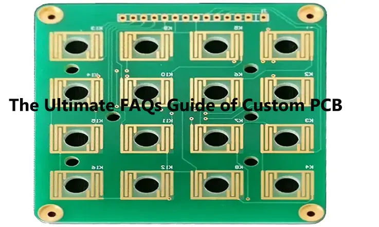
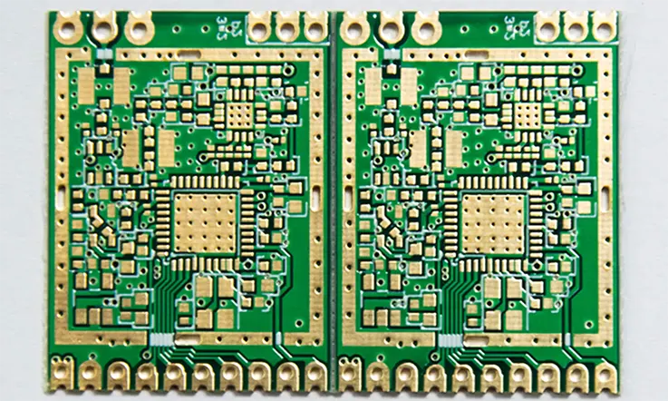
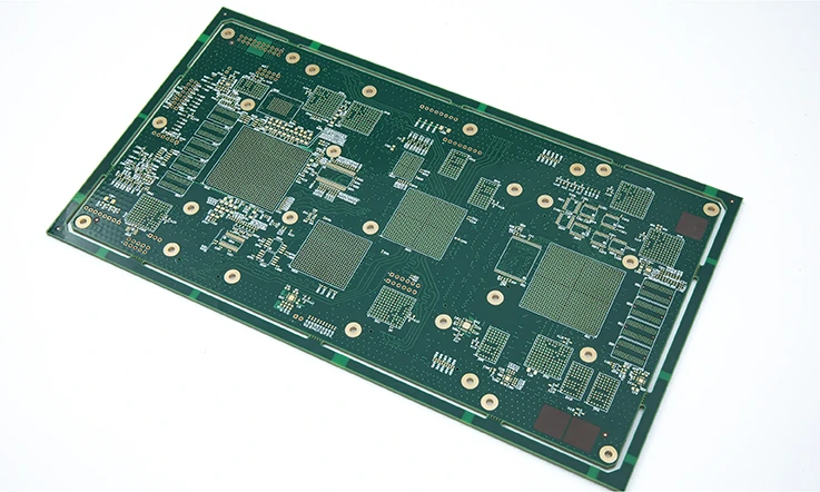
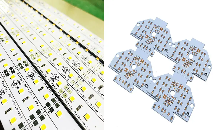
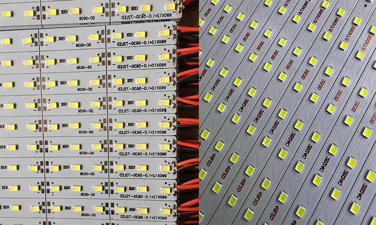
Printed Circuit Boards (PCBs) are a fundamental building block of electronic devices, providing a foundation for the interconnection and control of electronic components. Custom PCBs, also known as bespoke PCBs, are specifically designed to meet the precise requirements of an electronic device, such as size, functionality, and performance.
If you are considering importing custom PCBs, it is essential to familiarize yourself with the intricacies of this process. In this comprehensive guide, you will find detailed information about custom PCBs, including material selection, fabrication techniques, component mounting, hole drilling, and assembly procedures.
By perusing this guide, you will gain an in-depth understanding of custom PCBs, enabling you to make informed decisions about their design, manufacture, and implementation. Whether you are a seasoned professional or a newcomer to the field of electronics, this guide is an indispensable resource for achieving success in custom PCB development.
What is a Custom Printed Circuit Board?
A Custom Printed Circuit Board (PCB) is a circuit board that is designed and fabricated to meet specific requirements of an electronic device. It is tailored to the needs of the device and is not a standard, off-the-shelf product. Custom PCBs can be designed for both simple and complex electronic systems, and they offer numerous advantages over traditional, off-the-shelf PCBs.
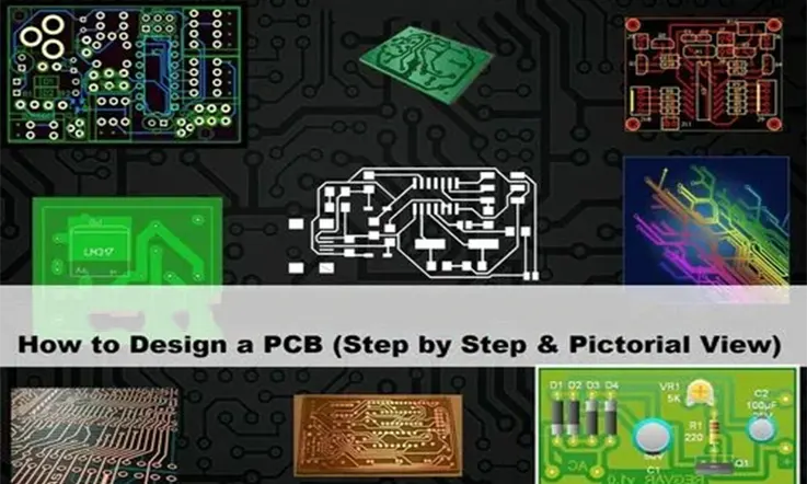
The process of designing a custom PCB involves understanding the specific requirements of the device, choosing the right software, capturing the schematic, designing the physical layout of the PCB, and running design rule checks. Once the design is complete, the custom PCB is fabricated using a manufacturing process that involves printing the design onto a substrate, etching the copper traces, drilling holes, and adding a solder mask and silkscreen layer.
How Many Types of Custom PCB?
There are several types of custom PCBs (Printed Circuit Boards) that can be designed and manufactured to meet specific requirements. Some of the most common types of custom PCBs include:
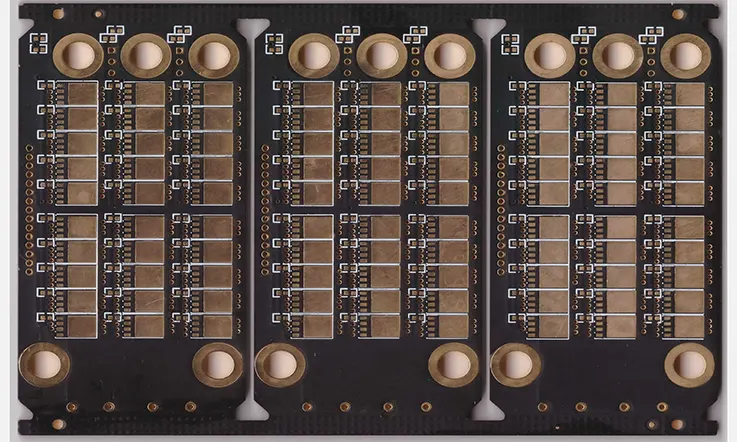
Single-layer PCBs: These PCBs have a single layer of conductive material on one side of the board.
Double-layer PCBs: These PCBs have conductive material on both sides of the board, with vias connecting the two layers.
Multilayer PCBs: These PCBs have multiple layers of conductive material separated by insulating layers.
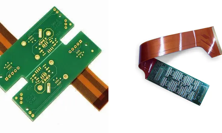
Flexible PCBs: These PCBs are made from flexible materials that can bend and conform to different shapes and sizes.
Rigid-Flex PCBs: These PCBs combine the advantages of rigid and flexible PCBs, with both rigid and flexible sections on the same board.
High-frequency PCBs: These PCBs are designed to operate at high frequencies and may use specialized materials and construction techniques.
High-density interconnect (HDI) PCBs: These PCBs use advanced manufacturing techniques to increase the density of components on the board.
The type of custom PCB that is best for a specific application will depend on the requirements of the project, such as the size and complexity of the circuit, the operating environment, and the performance specifications.
Benefits of Using Custom PCBs
The importance of custom PCBs lies in their ability to meet specific requirements of an electronic device and offer numerous advantages over traditional, off-the-shelf PCBs. The following are some of the key benefits of using custom PCBs:
Optimized performance
Custom PCBs can be designed to meet specific performance requirements, such as high-speed signaling, low noise, and low power consumption. Standard PCBs are designed to meet general requirements and may not be optimized for specific applications.
Space-saving
Custom PCBs can be designed to fit within the available space of the device, reducing the overall size of the device. This is particularly important for portable devices such as smartphones and tablets.
Cost-effective
Custom PCBs can be designed to reduce the number of components required, reducing the overall cost of the device. This is particularly important for high-volume production runs.
Improved reliability
Custom PCBs can be designed to improve the reliability of the device by reducing the risk of signal interference and noise. This is particularly important for critical applications such as medical devices and aerospace systems.
Faster time-to-market
Custom PCBs can be designed and fabricated more quickly than traditional, off-the-shelf PCBs. This enables designers to bring their products to market faster and stay ahead of the competition.
Overall, custom PCBs are an essential element in the design and development of electronic devices. They offer numerous advantages over traditional, off-the-shelf PCBs and enable designers to create products that meet specific requirements and perform optimally in their intended applications.
Which are the Disadvantages of Custom PCB ?
While custom PCBs offer many benefits, there are also some potential disadvantages to consider. Here are a few possible drawbacks of custom PCBs:
Higher cost: Custom PCBs are often more expensive to produce than standard off-the-shelf PCBs due to the additional design and manufacturing time required.
Longer lead time: Because custom PCBs require additional design and manufacturing time, they may take longer to produce than standard PCBs. This can be a disadvantage if there are tight deadlines for a project.
Higher risk of errors: Custom PCBs are more prone to errors than standard PCBs, as they are designed from scratch and may require more testing and refinement to ensure they work properly.
Limited availability: Custom PCBs may not be available from all PCB manufacturers, which can limit the options available to a designer.
Design complexity: Custom PCBs can be more complex to design, as they may require additional components or specialized features that are not available on standard PCBs.
Overall, while custom PCBs can be a great option for certain projects, it’s important to weigh the potential disadvantages against the benefits to determine whether they are the right choice for a particular application.
How to Design a Custom PCB ?
Designing a custom PCB involves several steps and requires a good understanding of the requirements of the electronic device. The following are the key steps in designing a custom PCB:
Understanding the design requirements
Before starting the design process, it is essential to understand the specific requirements of the electronic device. This includes determining the size and shape of the PCB, the number and type of components, the power requirements, and the desired performance characteristics.
Choosing the right software
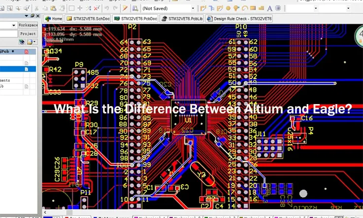
There are several software tools available for designing custom PCBs, such as Eagle PCB, Altium Designer, and KiCAD. The choice of software depends on the complexity of the design and the designer’s familiarity with the software.
Schematic capture
The schematic capture is the initial step in designing a custom PCB. It involves drawing the electrical circuit using symbols to represent electronic components and connecting them through wires.
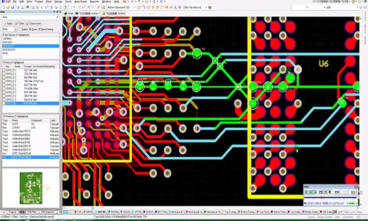
PCB layout
Once the schematic is complete, the next step is to design the physical layout of the PCB. This involves placing the components on the PCB and routing the connections between them.
Design rule checks
Before finalizing the design, it is essential to run design rule checks to ensure that the design meets the required specifications. These checks include verifying the spacing between components, the clearance between traces, and the minimum drill size.
By following these steps, a custom PCB designer can create a design that meets the requirements of the electronic device and ensures optimal performance.
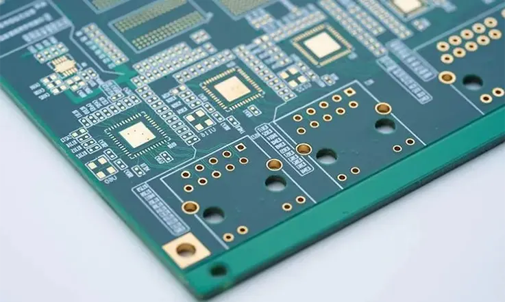
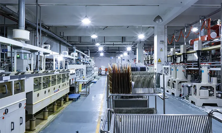
Custom PCB Fabrication Step
Custom PCB fabrication is the process of creating a printed circuit board (PCB) that is designed to meet specific requirements for a particular project or application. This process involves several steps, including designing the PCB layout, selecting the appropriate materials, and using specialized equipment to manufacture the board.
Here are some of the key steps involved in custom PCB fabrication:
1. Designing the PCB layout: The first step is to create a design for the PCB that meets the specific requirements of the project. This involves using PCB design software to create a schematic diagram of the circuit, which is then used to create the physical layout of the board.
2. Selecting the appropriate materials: The materials used in the fabrication process will depend on the specifications of the project. This may include selecting the appropriate substrate material, copper thickness, solder mask color, and other factors.
3. Creating the PCB artwork: Once the layout and materials have been determined, the next step is to create the artwork that will be used to manufacture the PCB. This involves using specialized software to create a file that contains all of the information needed to create the board.
4. Printing the artwork: The PCB artwork is then printed onto a special film that is used to create the PCB. This process is typically done using a specialized printer that is capable of producing high-quality images with fine details.
5. Manufacturing the board: Once the artwork has been printed, the PCB is manufactured using a process called etching. This involves using chemicals to remove the copper from the board in areas that are not part of the circuit. The board is then drilled and plated to create the necessary connections between components.
6. Quality control: After the board has been manufactured, it is inspected to ensure that it meets the required specifications. This may involve using specialized testing equipment to check for defects or errors in the circuit.
To sum up, custom PCB fabrication is a complex process that requires specialized knowledge and equipment. However, it can be an effective way to create high-quality PCBs that are tailored to meet the specific needs of a particular project or application.
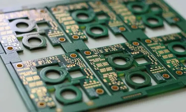
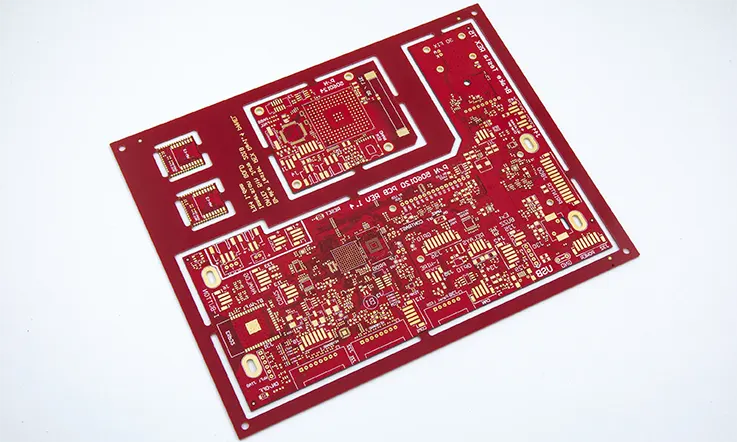
Which are the Main Materials Used in Custom PCB ?
There are several materials commonly used in the fabrication of custom PCBs, including:
Substrate materials: The substrate material is the base layer of the PCB and provides mechanical support for the circuitry. Common substrate materials include FR-4 (a type of fiberglass-reinforced epoxy), aluminum, and ceramic.
Copper foil: Copper foil is used to create the conductive pathways on the PCB. Copper foil is available in various thicknesses, and the choice of thickness will depend on the specific requirements of the project.
Solder mask: Solder mask is a protective layer that is applied over the copper traces to prevent solder from flowing where it’s not intended during assembly. The color of the solder mask is typically green, but other colors are also available.
Silkscreen: Silkscreen is a layer of ink that is applied over the solder mask to provide labeling and identification for the components on the PCB.
Surface finish: The surface finish is a coating that is applied to the exposed copper to protect it from oxidation and to improve the solderability of the PCB. Common surface finishes include HASL (hot air solder leveling), ENIG (electroless nickel immersion gold), and OSP (organic solderability preservatives).
Adhesive: Adhesive is used to bond the layers of the PCB together. The type of adhesive used will depend on the specific substrate material and the manufacturing process.
All in all, the choice of materials for a custom PCB will depend on the specific requirements of the project, including the desired performance characteristics, cost considerations, and manufacturing constraints. By carefully selecting the appropriate materials and manufacturing processes, it is possible to create a custom PCB that meets the required specifications and performs as expected.
What is DFM Checks in Custom PCB Fabrication ?
Design for Manufacturability (DFM) checks are a set of design guidelines used in the fabrication of custom printed circuit boards (PCBs) to ensure that the design is optimized for efficient and cost-effective manufacturing. These checks are performed by the PCB manufacturer to identify and address any design issues that could impact the quality or reliability of the finished product.
The DFM checks can include a review of the layout, component placement, routing, and other design elements to ensure that they are compatible with the manufacturing process and can be produced efficiently and accurately. By performing DFM checks, the manufacturer can help to ensure that the final product meets the intended specifications and is delivered on time and within budget.
Why is Drill Hole Size Tolerance Important During Fabrication of Custom PCB?
Drill hole size tolerance is an important consideration during the fabrication of custom PCBs because it can impact the performance and reliability of the finished product. The drill holes in a PCB are used to create connections between different layers of the board, and if the holes are not drilled to the correct size, it can result in a poor connection or even a complete failure of the PCB.
For example, if the drill holes are too small, it can make it difficult to insert the necessary components or to solder the connections, which can result in a weak or unreliable connection. On the other hand, if the drill holes are too large, it can lead to a loose or unstable connection, which can also impact the performance and reliability of the PCB.
To ensure that the drill holes are drilled to the correct size, it is important to specify the appropriate tolerance during the design phase of the PCB. This tolerance should take into account the specific requirements of the project and the capabilities of the manufacturing process, and should be verified during the quality control process to ensure that the finished product meets the required specifications.
Overall, drill hole size tolerance is an important consideration during the fabrication of custom PCBs, as it can impact the performance and reliability of the finished product. By specifying the appropriate tolerance and verifying it during the quality control process, it is possible to ensure that the finished product meets the required specifications and performs as expected.
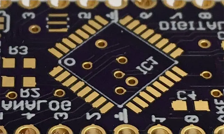
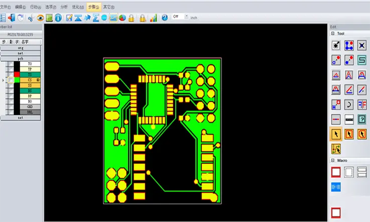
Which are the Different Types of Vias Used in Custom PCB ?
Vias are small holes that are drilled into a PCB and used to create connections between different layers of the board. There are several different types of vias commonly used in custom PCBs, including:
Through-hole vias: Through-hole vias are the most common type of via and are used to create connections between the top and bottom layers of the PCB. These vias are drilled all the way through the PCB and are plated with copper to create a conductive pathway.
Blind vias:Blind vias are drilled from the surface of the PCB down to an inner layer, but do not go all the way through the board. These vias are used to create connections between the outer layers and one or more inner layers of the PCB.
Buried vias: Buried vias are drilled between two inner layers of the PCB and do not extend to the outer layers. These vias are used to create connections between inner layers of the board without affecting the outer layers.
Microvias: Microvias are very small vias that are typically less than 0.15mm in diameter. These vias are used in high-density designs where space is limited.
Stacked vias: Stacked vias are multiple through-hole vias that are stacked on top of each other. These vias are used to create connections between multiple layers of the PCB.
Via-in-pad: Via-in-pad is a design technique where a via is placed directly under a component pad. This technique can help to save space and reduce signal noise.
Therefore, the choice of via type will depend on the specific requirements of the project, including the desired performance characteristics, cost considerations, and manufacturing constraints. By carefully selecting the appropriate via type and design, it is possible to create a custom PCB that meets the required specifications and performs as expected.
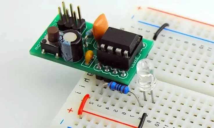
Do You Need a PCB Prototype when Developing Custom PCB ?
In most cases, it is a good idea to create a PCB prototype when developing a custom PCB. A prototype allows you to test and refine the design before moving on to full-scale production, which can help to identify and address any issues or errors in the design before they become bigger problems.
Creating a prototype can also help you to evaluate the performance of the PCB in real-world conditions and make any necessary adjustments to the design. This can be especially important in applications where reliability and accuracy are critical.
There are several methods for creating a PCB prototype, including using a breadboard or perfboard to create a simple prototype, or using a specialized PCB prototyping service to create a more advanced prototype.
Overall, while it may be possible to skip the prototype stage in some cases, it is generally recommended to create a prototype when developing a custom PCB to help ensure that the final product meets the intended specifications and performs as expected.
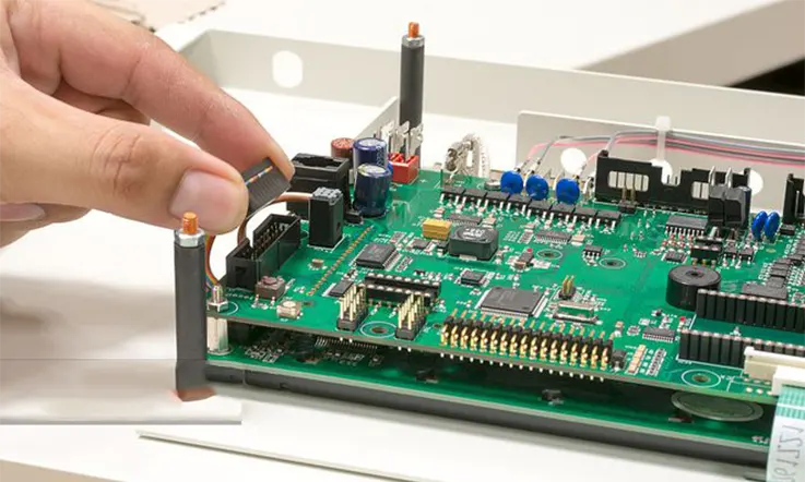
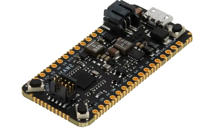
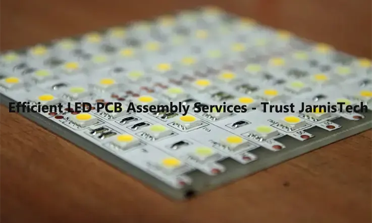
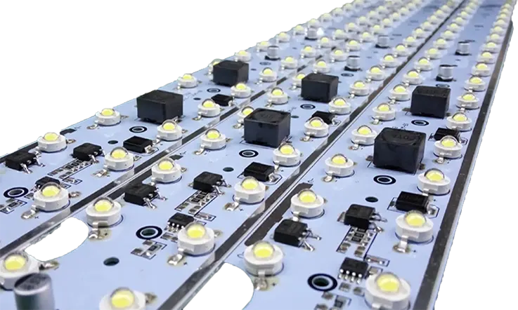
How Do You Assemble Custom PCB ?
Custom PCBs can be assembled using a variety of different methods, depending on the complexity of the design and the specific requirements of the project. Here are some of the most common methods for assembling custom PCBs:
Surface Mount Technology (SMT):SMT is a popular method for assembling custom PCBs, especially those with small components and high-density designs. SMT involves placing components directly onto the surface of the PCB and then soldering them into place using a reflow oven.
Through-Hole Technology (THT): THT involves inserting components through holes in the PCB and then soldering them onto the opposite side of the board. THT is commonly used for larger components and connectors that cannot be surface-mounted.
Mixed Technology: Mixed technology involves using both SMT and THT components on the same PCB. This method is often used when a design requires a combination of small and large components.
Automated Assembly: Automated assembly involves using robotic equipment to place and solder components onto the PCB. This method is often used for large-scale production runs, as it can help to improve efficiency and reduce costs.
Hand Assembly: Hand assembly involves manually placing and soldering components onto the PCB. This method is often used for small-scale or prototype production runs, as it can be more time-consuming and labor-intensive than automated assembly.
Overall, the method of assembling a custom PCB will depend on the specific requirements of the project, including the complexity of the design, the size of the components, and the volume of the production run. By carefully selecting the appropriate assembly method, it is possible to create a custom PCB that meets the required specifications and performs as expected.
When Should You Choose Custom PCBs ?
Custom PCBs are a good choice in a variety of situations, including:
1. When the project requires specific features or functionality that is not available on a standard PCB: Custom PCBs can be designed to include specialized features or functionality that may not be available on a standard PCB.
2. When the project requires a specific form factor or size: Custom PCBs can be designed to fit specific form factors or sizes, which can be important in applications where space is limited.
3. When the project requires a high level of precision or accuracy: Custom PCBs can be designed to very precise specifications, which can be important in applications where accuracy is critical.
4. When the project requires a high level of reliability or durability: Custom PCBs can be designed with materials and manufacturing processes that are optimized for reliability and durability, which can be important in applications where the PCB will be subjected to harsh environments or rough handling.
5. When the project requires a high level of customization or personalization: Custom PCBs can be designed to include personalized branding, logos, or other custom features that can help the project stand out.
As a result, custom PCBs are a good choice when the project requires specific features, functionality, form factors, or levels of precision or reliability that are not available on a standard PCB. It’s important to weigh the potential benefits of custom PCBs against the potential drawbacks, such as higher cost and longer lead times, to determine whether they are the right choice for a particular application.
Why Conformal Coating is Your Custom PCB Option?
Conformal Coating, also known as three-proof adhesive, insulating adhesive, moisture-proof agent, moisture-proof oil, protective paint, or protective paint, is a specialized coating that provides protection to electronic components. While it is commonly associated with preventing moisture, mold, and salt spray (the “three anti” function), its protective capabilities extend far beyond that.
In addition to its moisture-resistant properties, Conformal Coating provides protection against dust, friction, shock, high temperatures, and chemical environments. It also helps prevent PCB circuit board failure, enhances insulation strength, and extends the life of the circuit board.
When applied, Conformal Coating creates a dense protective film on the surface of the PCB, effectively shielding the circuit from environmental erosion. As a result, it is an indispensable component in ensuring the longevity and reliability of electronic devices.
How to Choose the Reliable Custom PCB Manufacturer ?
Choosing a reliable custom PCB manufacturer is an important step in ensuring the quality and performance of your PCBs. Here are some factors to consider when choosing a custom PCB manufacturer:
1. Experience and Reputation: Look for a manufacturer with a proven track record of producing high-quality PCBs. Check their website for customer reviews and testimonials, and see if they have experience in manufacturing PCBs for your specific industry or application.
2. Quality Control: Ask about the manufacturer’s quality control processes and certifications. Look for a manufacturer that uses high-quality materials, performs rigorous testing, and has certifications such as ISO 9001 or UL.
3. Technical Expertise: Ensure that the manufacturer has the technical expertise to handle your project’s requirements. Ask about their experience with the specific materials, components, and manufacturing processes needed for your project.
4. Customer Service: Look for a manufacturer that provides excellent customer service, including clear communication, fast response times, and a willingness to work with you to resolve any issues that may arise.
5. Pricing and Lead Times: Compare pricing and lead times from multiple manufacturers to ensure that you are getting a competitive price and a realistic production timeline.
6. Location and Shipping: Consider the location of the manufacturer and their shipping options. A manufacturer located closer to your facility may offer faster shipping times and lower shipping costs.
By considering these factors, you can choose a reliable custom PCB manufacturer that can provide high-quality, cost-effective PCBs for your project.
Why Choose Jarnistech Custom PCBs ?
For more than two decades, we have been a leading manufacturer of custom PCBs, catering to diverse industries. Our custom PCBs are designed with cutting-edge features that can elevate the performance of your applications significantly.
At JarnisTech, we prioritize delivering custom PCBs of the highest quality. Our team adheres to industry best practices to ensure that the PCBs we manufacture are tailored to meet your specific requirements and fully functional.
We understand the importance of precision and reliability in PCB manufacturing, and we employ the latest techniques and technologies to guarantee that your boards will fit your applications perfectly. With our custom PCBs, you can rest assured that you are getting a top-of-the-range product that will enhance the quality and performance of your applications.
FAQ Section of Custom PCBs
Here are some common questions and answers related to custom PCBs:
Q: How much does a custom PCB cost?
A: The cost of a custom PCB will depend on several factors, including the complexity of the design, the materials used, and the volume of the order. Generally, custom PCBs are more expensive than standard off-the-shelf PCBs due to the additional design and manufacturing time required.
Q: How long does it take to make a custom PCB?
A: The lead time for a custom PCB will depend on several factors, including the complexity of the design, the materials used, and the volume of the order. Generally, custom PCBs take longer to produce than standard off-the-shelf PCBs due to the additional design and manufacturing time required.
Q: What are some common mistakes to avoid when designing a custom PCB?
A: Some common mistakes to avoid when designing a custom PCB include not leaving enough space between components, not following design rules for the specific PCB manufacturer being used, and not properly testing the design before manufacturing.
Q: What industries and fields use custom PCBs?
A: Custom PCBs are used in a wide range of industries and fields, including aerospace, automotive, medical, telecommunications, and consumer electronics, among others.
Q: What software is used to design custom PCBs?
A: There are many software tools available for designing custom PCBs, including Altium Designer, Eagle PCB, KiCAD, and others.
Q: What materials are commonly used in custom PCB fabrication?
In such situations, it is possible to reverse engineer a custom PCB, but it can be a difficult and time-consuming process. Reverse engineering involves analyzing the design of the PCB to determine its functionality and how it was created. This can involve using specialized equipment to examine the PCB under a microscope, analyzing the layout and component placement, and tracing the circuitry to determine its function.
Q: What is the difference between a through-hole and surface-mount component?
A: Through-hole components have leads that are inserted through holes in the PCB and soldered on the other side, while surface-mount components are soldered directly to the surface of the PCB. Surface-mount components are generally smaller and more compact than through-hole components.
These are just a few examples of common questions related to custom PCBs. If you have specific questions related to your project or application, it’s best to consult with a JarnisTech PCB manufacturer or engineer to get more personalized advice and guidance.
Conclusion
Custom PCBs are an essential component in modern electronics design and manufacturing. They enable precise control and measurement of electrical signals, allow for compact and high-performance circuitry, and can be tailored to specific product requirements. Custom PCBs are used in a wide range of industries and fields, including consumer electronics, medical devices, aerospace and defense, industrial automation, automotive, and Internet of Things (IoT) devices.
With the ability to design and manufacture PCBs to specific requirements, custom PCBs offer endless possibilities for innovation and product development. Whether you are working on a new consumer product, medical device, or industrial automation system, custom PCBs can be an invaluable tool for bringing your ideas to life.
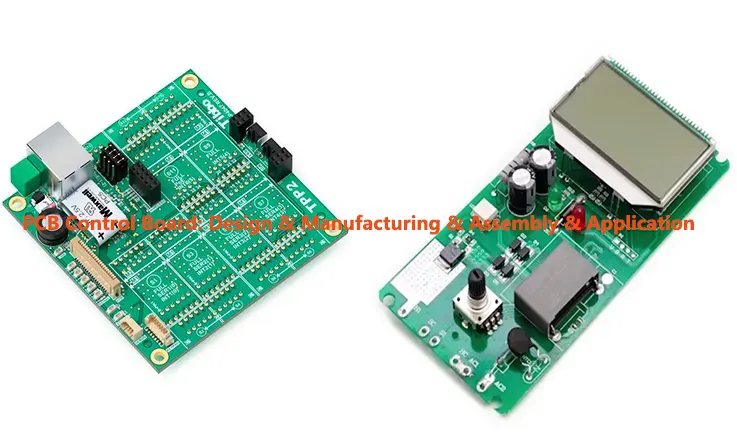
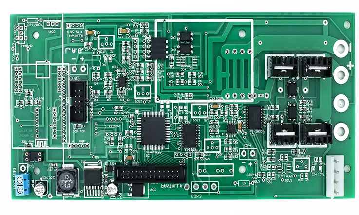
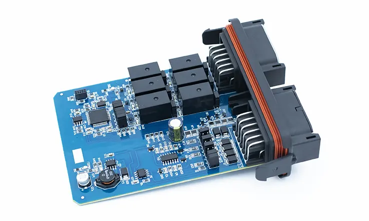
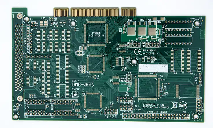
A PCB control board, also known as a printed circuit board control board, is a critical component in electronic devices that controls and manages the flow of signals and power between different components on the board. It is responsible for regulating the operation of the device and ensuring that it functions correctly.
The PCB control board provides a stable and reliable platform for electronic components to be mounted and connected, reducing the risk of loose connections or short circuits. It is an essential component in modern electronics, contributing to the efficiency and reliability of electronic devices.
The importance of the PCB control board lies in its ability to provide a standardized platform for electronic components and circuits. By using a PCB control board, manufacturers can streamline the design and production process, reduce costs, and improve the overall quality of their products. Additionally, the use of PCB control boards allows for easier repair and maintenance of electronic devices, as individual components can be easily replaced or upgraded.
PCB Control Board Basics
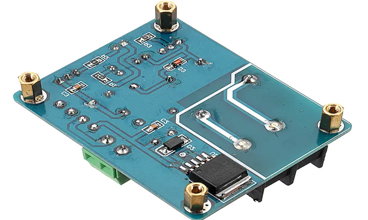
The PCB control board is a type of printed circuit board that contains electronic components and circuits that are designed to control and manage the flow of signals and power in electronic devices. It is an essential component in most modern electronic devices, from simple household appliances to complex industrial systems.
The basic structure of a PCB control board consists of a substrate material, typically made of fiberglass or plastic, with a thin layer of copper foil laminated onto it. The copper layer is etched to create a pattern of conductive traces that connect the various electronic components on the board. The conductive traces are arranged in a specific layout, called a circuit or circuitry, that enables the control board to perform its intended function.
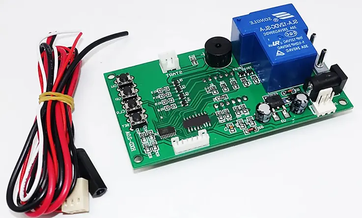
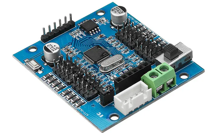
The electronic components that are mounted on the PCB control board include resistors, capacitors, diodes, transistors, and integrated circuits, among others. These components are soldered onto the board to form the circuitry. The PCB control board may also include connectors, switches, and other components that allow it to interface with other electronic devices.
The design of a PCB control board is critical to its performance and reliability. The layout of the conductive traces must be optimized to minimize interference and signal loss, while the placement of components must be carefully considered to ensure that the board can operate within its specified temperature and power requirements.
Overall, understanding the basics of the PCB control board is essential for anyone involved in the design, manufacture, or repair of electronic devices. By mastering the principles of PCB control board design, engineers and technicians can create more efficient, reliable, and high-quality electronic products.
What are Materials used to manufacturing PCB Control Board ?
The materials used in the manufacturing of PCB control boards can vary depending on the specific requirements of the application, but typically include the following:
Substrate materials: The substrate material is the base material on which the conductive traces and pads are etched. Common substrate materials used in PCB manufacturing include fiberglass-reinforced epoxy (FR-4), polyimide, and Rogers.
Copper foil:Copper foil is used to create the conductive traces and pads on the substrate. The thickness of the copper foil can vary depending on the required current-carrying capacity and resistance.
Solder mask:Solder mask is a protective coating applied over the copper traces to prevent solder from adhering to areas where it is not desired.
Silkscreen:Silkscreen is a labeling system that is printed onto the board to identify components, test points, and other important features.
Surface finish: The surface finish is a coating applied to the exposed copper on the board to prevent oxidation and improve solderability. Common surface finishes include HASL (hot air solder leveling), ENIG (electroless nickel immersion gold), and OSP (organic solderability preservative).
Adhesive:Adhesive is used to bond layers of the board together and to hold components in place during assembly.
Overall, the materials used in the manufacturing of PCB control boards must be carefully selected to ensure that they meet the required specifications for performance, reliability, and manufacturability. By choosing the right materials and following best practices in PCB design and manufacturing, manufacturers can ensure that their PCB control boards are of the highest quality and meet the needs of the intended application.
Design and Routing Considerations of PCB Control Board
The layout and routing of a PCB control board are critical steps in the design process that determine the performance, reliability, and manufacturability of the board. Here are some key factors to consider when laying out and routing a PCB control board:
Trace routing: Conductive traces should be routed in a way that minimizes signal loss, reduces noise, and maintains signal integrity. This can be achieved by using proper trace widths, spacing, and routing patterns, as well as by using ground planes and signal layers.
Power requirements: One of the most critical design considerations for a PCB control board is determining the power requirements of the circuitry and ensuring that the board can handle the required voltage and current levels. Designers must carefully select the appropriate power supply components, such as voltage regulators and capacitors, and ensure that they are placed correctly on the board.
Signal integrity: Another critical design consideration is ensuring that the conductive traces on the PCB control board have low impedance and minimal signal loss. This can be achieved by carefully selecting trace widths, spacing, and routing patterns, as well as using proper grounding techniques.
Component placement: The placement of electronic components on the PCB control board is also essential. Components must be arranged in a way that minimizes interference and signal crosstalk, while also allowing for efficient heat dissipation and easy access for maintenance and repair.
Thermal management: The PCB control board must be designed to handle the heat generated by electronic components during operation. This can be achieved by using adequate heat sinks, thermal vias, and other cooling components.
Manufacturing considerations: The design of the PCB control board must also take into account the limitations and capabilities of the manufacturing process. Designers must ensure that the board can be manufactured efficiently and cost-effectively, while also meeting all quality and reliability standards.
EMI/EMC compliance: The PCB control board must comply with electromagnetic interference (EMI) and electromagnetic compatibility (EMC) regulations to prevent interference with other electronic devices and ensure that the device operates reliably.
Design for manufacturability: The layout and routing of the board should be designed to facilitate the manufacturing process. This includes considerations such as panelization, fiducials, and proper spacing between components.
As a result, the design of the layout and routing of the PCB control board should take into account the specific requirements of the intended application, as well as the limitations of the manufacturing process. By carefully considering these factors, designers can create a highly efficient, reliable, and manufacturable PCB control board.
PCB Control Board: Manufacturing and Assembly
The manufacturing and assembly of a PCB control board involves several critical steps that determine the quality and reliability of the final product. Here are some of the key steps involved in manufacturing and assembling a PCB control board:
PCB fabrication: The first step in the manufacturing process is to fabricate the PCB itself. This involves several steps, including drilling, plating, and etching the board to create the conductive traces and pads.
Solder paste application: Once the board is fabricated, solder paste is applied to the pads on the board using a stencil. The paste is a mixture of solder and flux that helps to hold the components in place during assembly.
Component placement: Electronic components are then placed on the board using automated pick-and-place machines. The components are aligned with the pads on the board and held in place by the solder paste.
Soldering: The board is then moved into a reflow oven, where the solder paste is heated and melted to create a permanent bond between the components and the board. This process is called surface mount technology (SMT) soldering.
Through-hole components: If the design includes through-hole components, they are inserted into the board and soldered using wave soldering or hand-soldering techniques.
Inspection and testing: After assembly, the board is inspected for defects, such as solder bridges, missing components, and misaligned components. The board is then tested to ensure that it meets the required specifications for performance and reliability.
Final packaging: Once the board has passed inspection and testing, it is packaged and prepared for shipment to the customer or for use in the final product assembly.
In a word, the manufacturing and assembly of a PCB control board require a high degree of precision and attention to detail. By following best practices for PCB assembly and testing, manufacturers can ensure that the final product is of the highest quality and meets the required specifications for performance and reliability.
Testing and Quality Control of Control Circuit Board
Testing and quality control are critical steps in the manufacturing process of a PCB control board. Here are some of the key steps involved in testing and quality control:
Visual inspection: The board is visually inspected to check for any defects, such as missing components, incorrect placement, or soldering defects.
Functional testing: The board is tested to ensure that it functions as intended. This can include testing for electrical continuity, signal quality, and power consumption.
Environmental testing: The board is tested under various environmental conditions, such as temperature and humidity, to ensure that it can withstand the conditions it will be exposed to in its intended application.
Electrical testing: The board is tested using specialized equipment to measure its electrical characteristics, such as impedance, capacitance, and resistance.
Reliability testing: The board is subjected to various stress tests to assess its reliability and durability. These tests can include thermal cycling, vibration, and shock testing.
Quality control documentation: All testing results and quality control procedures are documented to ensure traceability and accountability throughout the manufacturing process.
To sum up, testing and quality control are critical steps in ensuring that a PCB control board meets the required specifications for performance and reliability. By following rigorous testing procedures and documenting all results and procedures, manufacturers can ensure that the final product is of the highest quality and meets all required standards.
Control PCB Board Application
PCB control boards are used in a wide range of electronic devices and applications, including:
Consumer electronics
PCB control boards are used in a variety of consumer electronics, such as smartphones, laptops, televisions, and home appliances, to control the flow of signals and power between different components.
Industrial automation
PCB control boards are used in industrial automation systems to control and monitor the operation of machinery, equipment, and processes.
Automotive
PCB control boards are used in automotive applications to control the operation of various systems, such as the engine, transmission, and braking systems.
Aerospace
PCB control boards are used in aerospace applications to control the operation of various systems, such as flight control systems, navigation systems, and communication systems.
Medical devices
PCB control boards are used in medical devices, such as diagnostic equipment and monitoring systems, to control the flow of signals and power between different components.
Military and defense
PCB control boards are used in military and defense applications to control the operation of various systems, such as communication systems, radar systems, and weapon systems.
Overall, PCB control boards are an essential component in modern electronics, contributing to the efficiency, reliability, and functionality of electronic devices in a wide range of applications.
How to Choose a High Quality PCB Control Board Fabricator?
Choosing a high-quality PCB control board fabricator is crucial to ensure that your electronic device operates efficiently and reliably. Here are some tips to help you choose a reputable and reliable PCB fabricator:
Look for experience: A PCB fabricator with years of experience in the industry is more likely to have a good understanding of the manufacturing process and can produce high-quality PCBs consistently.
Check certifications: Ensure that the PCB fabricator has the necessary certifications and meets industry standards such as ISO 9001, UL, and RoHS compliance.
Quality control processes: A reliable PCB fabricator should have strict quality control processes in place to ensure the PCBs are manufactured to the required specifications and standards.
Technical support: Look for a PCB fabricator that offers technical support and assistance during the design and manufacturing process to help identify and resolve any issues that may arise.
Production capacity: Consider the production capacity of the PCB fabricator. A fabricator with a large production capacity can handle large orders and can deliver the PCBs on time.
Cost: While cost is an important factor, it should not be the only consideration. Choosing a fabricator based solely on cost can result in lower quality PCBs that may not meet your requirements.
Reviews and referrals: Check online reviews and ask for referrals from other customers to get an idea of the fabricator’s reputation and the quality of their work.
By considering these factors, you can choose a high-quality PCB control board fabricator that meets your needs and produces reliable and efficient PCBs for your electronic devices.
Why Choose Us?
JarnisTech – 20 Years Experience PCB Control Board Manufacturer
Jarnistech is a reputable manufacturer that specializes in the production of high-quality PCB control boards for over 20 years. We are committed to providing our clients with the best quality products that meet their business requirements.
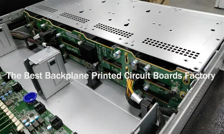
Our PCB control boards are available in a wide range of designs and configurations. They are designed with advanced features that ensure high reliability in connecting multiple PCBs. We have a team of highly skilled and knowledgeable engineers who are experts in component sourcing, fabrication, assembly, and production of PCB control boards. Our engineers use advanced manufacturing technology to produce products that meet the highest quality standards.
Our PCB control boards are large printed circuit board formats that serve as a backbone for connecting various PCBs to form a computer bus. We also manufacture PCB control boards that function as a connection between active PCBs. Our products feature high mechanical stability and strength, high-signal integrity design, controlled impedance, buried vias, back drilling, and high speed.
At Jarnistech, we understand the importance of customer satisfaction, and we strive to provide our clients with the highest level of satisfaction. We offer competitive prices and low MOQ to support starting businesses. All our products have qualifications from ISO9001, ISO14000, UL, and more. We do not compromise on the quality of our products, and we guarantee high-quality PCB control boards.
Apart from PCB control boards, we also manufacture Rogers 3003, Rogers 5880, Rogers 4360, Rogers 3006, Rogers 3010, IC Substrate, Surface finish PCB, Flex PCB assembly, Power supply PCB, Inverter PCB, and more. Jarnistech is your one-stop solution for your PCB needs.
Choose Jarnistech as your number one supplier of high-quality PCB control boards. We are an expert in manufacturing authentic and genuine products that meet the highest quality standards. Our wide range of PCB control boards will surely meet your requirements.
Conclusion
PCB control boards are a critical component in modern electronic devices, providing the necessary control and signal routing to ensure their proper operation. Designing and manufacturing a high-quality PCB control board requires careful consideration of factors such as power requirements, signal integrity, component placement, thermal management, manufacturing considerations, and EMI/EMC compliance.
The layout and routing of the board must also be carefully designed to ensure efficient signal flow and minimal interference. Manufacturing and assembly involve several critical steps, including PCB fabrication, component placement, soldering, inspection and testing. Quality control procedures are essential to ensure that the final product meets the required specifications for performance and reliability.
PCB control boards have a wide range of applications in consumer electronics, industrial automation, automotive, aerospace, medical devices, military, and defense. By following best practices in PCB design, manufacturing, and testing, manufacturers can ensure that their PCB control boards are of the highest quality and contribute to the efficiency and reliability of electronic devices.
Castellation PCB technology has become a prevalent assembly technique in the fabrication of PCBs. Its usage is steadily increasing due to the myriad advantages it offers. With the rapid advancement of modern technologies, the demand for Castellation PCB is also on the rise.
JarnisTech, a distinguished PCB manufacturing company, is renowned for its unwavering dedication to delivering products of the highest quality. Our PCBs are trusted and employed across more than 60 countries worldwide. We take pride in leveraging cutting-edge technologies to manufacture PCBs that consistently embody excellence.
Should you seek comprehensive knowledge on Castellation PCB, we invite you to explore our informative FAQ guide. It covers all aspects relevant to castellated PCB, serving as a valuable resource to address your inquiries. We encourage you to peruse its contents and gain a thorough understanding of the benefits and functionality of castellated PCB technology.
What Is A Castellation PCB ?
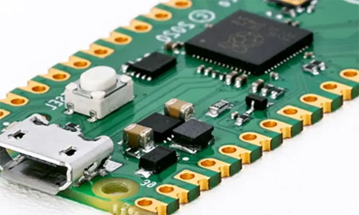
A castellated PCB, also known as a castellated module or castellation board, is a type of printed circuit board (PCB) that features small notches or cuts along the board’s edges, creating a pattern of interlocking teeth. These teeth make it easier to integrate the board with other components or boards, making it a popular choice for electronic devices and modules.
Castellated PCBs are commonly used in applications such as RF modules, Bluetooth modules, and Wi-Fi modules. They can also be used in sensors, cameras, GPS modules, and other electronic devices that require a compact design and easy integration.
Castellated PCBs are typically designed with surface-mount technology (SMT) components, which allow for a smaller footprint and more efficient use of space. They can be manufactured using standard PCB manufacturing techniques, but require additional care during assembly and testing to ensure that the interlocking teeth are properly aligned and secured.
Overall, castellated PCBs offer a versatile and efficient solution for electronic designers who need to integrate multiple components into a small space, while maintaining a secure and reliable connection.
Characteristics Of Castellation PCB
Castellation PCBs have several unique characteristics that make them a popular choice for electronic designers. Here are some of the key characteristics of castellation PCBs:
Interlocking teeth: Castellation PCBs feature small notches or cuts along the board’s edges, creating a pattern of interlocking teeth that allow the board to be easily integrated with other components or boards.
Compact design: Castellation PCBs are designed to be compact, making them ideal for applications where space is limited. They can be used in devices such as sensors, cameras, and GPS modules.
Surface-mount technology (SMT): Castellation PCBs are typically designed with surface-mount technology (SMT) components, which allow for a smaller footprint and more efficient use of space.
Multipurpose: Castellation PCBs can be used in a wide range of applications, including RF modules, Bluetooth modules, Wi-Fi modules, and other electronic devices that require a compact design and easy integration.
Manufacturing: Castellation PCBs can be manufactured using standard PCB manufacturing techniques, but require additional care during assembly and testing to ensure that the interlocking teeth are properly aligned and secured.
Easy integration: The interlocking teeth of castellation PCBs make it easy to integrate the board with other components or boards, reducing the need for additional connectors or cables.
Design Considerations for Castellation PCBs
When undertaking the design of a castellated board, it is imperative to prioritize both high yield and superior quality. The intricate process of designing a castellated circuit necessitates a thorough approach, particularly in relation to designing castellated pads. It is crucial to acknowledge that this process is complex and demands careful attention as even a single costly mistake has the potential to detrimentally impact the overall performance of the circuit board. Consequently, a comprehensive understanding of essential considerations is required for effective castellated pad design.
Half hole PCB
When designing a castellation for a half hole board, PCB designers must be mindful of certain crucial factors. Here are key considerations to bear in mind:
Holes with smaller lead-in holes:
● These holes are highly suitable for connector applications and can be created using a cutting tool. Additionally, they facilitate the creation of smaller castellations as necessary.
Utilize the bottom and top edge for hole placement:
● To ensure the circuit board remains firmly in place, it is recommended to avoid using the vertical edges as locations for the holes. These edges typically serve as bridges, and utilizing them could compromise the stability of the board.
It is important to note that there are various designs available for half holes, which can differ based on the software employed in the design process.
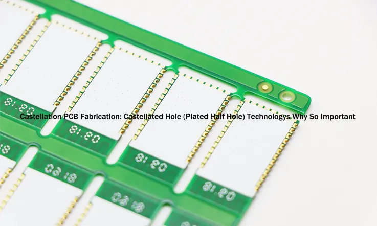
What is Castellated Hole (Plated Half Hole PCB) ?
Castellated holes, also known as castellations, are semi-plated indentations located on the edges of a PCB board. They serve the purpose of facilitating the mounting of one PCB board onto another, streamlining the assembly process. Depending on the specific application, these holes may take on the form of partial circles, enabling precise alignment between the two boards.
The presence of castellated holes ensures proper soldering of the boards, particularly in board-to-board soldering processes. These castellations are commonly utilized in various PCB modules, such as Wi-Fi or Bluetooth modules. Despite being separate components, these modules can be mounted together through soldering, facilitated by the castellated holes. This direct connection between two PCBs results in a noticeably slim system, in contrast to bulkier multi-pin connectors.
During PCB assembly processes, Through-Hole Technology and Surface Mount Technology are widely employed. Board-to-board soldering is a common practice when there is a requirement to mount two PCB boards together. Castellated holes play a pivotal role in establishing the connection between the board and the module, bridging the gap between them.
How Many Method to Make Castellated Holes ?
Castellated holes or vias are formed through a standard via process involving the drilling of holes and subsequent copper plating. These holes, shaped like semi-circles, are strategically created on the edges of the PCB by cutting through the board to form partial or half holes. This process allows for openings to be established along the board edges, giving rise to the distinctive appearance of castellated holes. It is worth noting that there exist multiple methods to achieve the creation of castellated holes.
Half Holes
Holes with Smaller cut-in Half Holes
Holes with smaller lead-in holes for post-processing: They are designed for connector applications.
In the production process of metalized castellated holes, there have been persistent challenges regarding manufacturing defects like copper plating peeling and warping. These defects can lead to unstable solder connections both physically and electrically. In extreme cases, they can also result in short circuits between adjacent pads.
The drilling and plating of castellated holes follow the same procedure as standard plated through holes (PTHs). However, the critical aspect lies in safely removing the opposite half of each hole without damaging the first half or leaving excess copper behind.
JarnisTech, a renowned PCB manufacturer, has developed a detailed process for castellated holes. We ensure that all drill and milling bits approach the board from the correct side while rotating in a clockwise direction. This careful approach guarantees that the copper plating remains pressed against the backing wall during the cutting process. As a result, the unwanted half of the copper ring is cleanly and accurately removed while leaving the other half intact. JarnisTech, the company behind the castellated hole process, has achieved a high level of refinement in our technique.
It is important to note that manufacturing castellated holes is more complex compared to standard PTHs, requiring precision and meticulous handling. Due to the additional drilling process and the often small nature of castellated boards, their production tends to be more expensive.
Stacking Conditions of Castellated Holes
In the realm of PCBs, the term “PCB stack-up” refers to the arrangement of insulating and copper layers that constitute a PCB. The chosen stack-up configuration significantly impacts the performance of the board.
Castellated holes play a crucial role in the process of PCB stack-up. Creating castellated mounting holes is an effective means of manufacturing PCBs intended to be stacked on top of one another. These holes contribute to achieving an excellent printed circuit board stack-up.
It is important to recognize that specific conditions must be met for successful PCB stack-up. Firstly, there should be no gaps or spacing between the two PCBs. The presence of gaps would hinder proper stacking conditions. Secondly, electrical connectivity is essential, going beyond mere physical attachment. Lastly, it is assumed that the size of the upper PCB is approximately one-third that of the bottom PCB.
The aforementioned conditions outline the requirements for castellated-hole-based stacking methods. They provide a foundation for realizing successful PCB stack-up.
Recommended Specifications for Castellated Holes
When incorporating castellated holes in PCB design, it is advisable to adhere to certain recommended specifications:
Size: Utilizing the largest available size for the castellated holes is beneficial as it facilitates proper PCB mounting, ensuring a secure fit.
Pad design: Opting for the largest pad size for each castellation is preferable as it allows for improved compatibility and alignment during assembly.
Distance and diameter: Half holes are suitable for both standard and advanced circuit boards. For standard circuit boards, a minimum hole diameter of 0.6mm is recommended, while for more advanced boards, a smaller diameter can be utilized. Furthermore, it is essential to maintain a minimum distance of 0.55mm between two castellations.
Surface finish: The choice of surface finish plays a significant role in achieving accurate PCB mounting. Electroless Nickel Immersion Gold (ENIG) finish is widely regarded as an excellent option for circuit boards. However, the specific application of the PCB should be considered when determining the most suitable surface finish.
Adhering to these design specifications for castellated holes contributes to the overall effectiveness and functionality of the PCB, ensuring successful mounting and optimal performance.
How to Fabricate a Circuit Board Castellated Pads ?
Here are the steps to fabricate a circuit board with castellated pads:
1. Design the circuit: Design the circuit schematic as per your requirement and choose the appropriate software for PCB design, such as Eagle, Altium, KiCad, or any other of your choice.
2. Define the board outline: Define the board outline with the castellations. This can be done by drawing a line across the board where you want the castellations to be.
3. Add castellations: Once the board outline is defined, add castellations to the board edges by creating small notches or cuts along the edge of the board.
4. Define the copper pour area: Define the copper pour area around the castellations. This will help to create a secure connection between the PCB and other components.
5. Place components: Place the components on the board as per the schematic. Make sure to keep the castellated edge in mind while placing components.
6. Generate Gerber files: Once the design is complete, generate the Gerber files for the PCB manufacturer.
7. PCB manufacturing: The manufacturer will use the Gerber files to manufacture the PCB with castellations.
8. Solder mask: Apply a solder mask over the entire board surface, including the castellations.
9. Copper plating: Apply copper plating on the castellations to make them conductive.
10. Remove the solder mask: Remove the solder mask from the castellations using a laser or chemical etching process.
11. Finish the board: Finish the board by adding components, testing for functionality, and applying a final coat of protective finish.
Overall, fabricating a circuit board with castellated pads requires additional care during the manufacturing process to ensure that the castellations are properly plated and secure. It’s recommended to consult with a manufacturer or expert in PCB design to ensure the board meets your specific requirements and standards.
So Why Castellated Hole (Plated Half Hole) Technology Is Important
Castellated holes on PCBs offer several advantageous features:
Surface mounting: Castellated holes provide a convenient mechanism for surface mounting the PCB onto another PCB or device. The exposed pins can be directly soldered to the required component, eliminating the need for connectors or extra hardware.
Space-saving: The compact and space-saving design of castellated holes is particularly useful in applications where space is limited or when a low-profile connection between PCB boards or components is desired.
Simplified assembly: Castellated holes streamline the assembly process by reducing the requirement for separate connectors or mounting hardware. This simplification can effectively reduce both assembly time and expenses.
Robust mechanical connection: Castellated holes offer a strong and reliable mechanical connection between the PCB and the component. The plated pins provide increased stability and durability compared to other surface-mounting techniques.
Electrical connectivity: The castellated pins establish a dependable electrical connection between the PCB and the components. This direct conductive path ensures proper signal transmission and reduces the risk of signal degradation or interference.
Design flexibility: Castellated holes grant designers greater flexibility, enabling the creation of unique PCB board form factors and supporting innovative product designs. The positioning of the castellated holes at specific locations along the board edge can be tailored to meet specific requirements.
Cost-effective solution: By reducing the need for connectors or additional mounting hardware, castellated holes can contribute to overall cost savings in manufacturing processes. The simplicity of the design and assembly processes can potentially provide a more cost-effective solution.
What Are The Ways To Achieve A PerfectCastellation PCB?
To ensure optimal mechanical strength in a Castellation PCB, several factors should be carefully considered:
Break tabs: Incorporating break tabs is essential to enhance mechanical stability during the board’s manufacturing and assembly. Break tabs with an edge length of up to 5mm, positioned at two locations per edge, help secure the panel to the PCB. The specific positioning and quantity of break tabs depend on the board’s shape and size.
Copper annular rings: It is advisable to utilize copper annular rings on both the upper and back sides of the Castellation PCB. The minimum pad size should match the finished hole size, ensuring sufficient mechanical stability.
Consistent pad sizes: Maintaining consistent pad sizes on the inner layers and matching sizes in the surface layers at the annular rings is crucial. This uniformity in pad sizes contributes to increased mechanical stability throughout the Castellation PCB.
ENIG surface finish: Selecting Electroless Nickel Immersion Gold (ENIG) as a surface finish improves the functionality of the castellated PCB, regardless of its size. ENIG allows for a reduction in required diameters, optimizing the mechanical performance of the PCB.
Half-hole configuration: Ensuring that half of the hole remains on the castellated PCB is a prudent practice. Deviating from this ratio may increase the potential for manufacturing faults and compromise mechanical stability.
To sum up, allocating space for break tabs, utilizing generous annular rings, opting for ENIG surface finish, and maintaining the half-hole configuration all contribute to achieving superior mechanical stability and reliability in Castellation PCBs.
Conclusion
Having gone through the information presented, you have now gained a clear understanding of the significance of castellated holes in various industries, such as industrial control, automobiles, telecommunications, and computer applications. If you are considering projects involving castellated holes or seeking to leverage castellated hole technology in the production of castellation PCBs, we are here to assist you.
We possess comprehensive knowledge of the manufacturing process and stacking conditions associated with half-hole PCBs. Our expertise will ensure the delivery of high-quality castellated holes that align perfectly with your system requirements.
Furthermore, our products are manufactured to meet rigorous quality standards, including ISO9001, RoHS, and UL. If you are in need of exceptional castellated holes for your designs, we are eager to provide our assistance. Rest assured that we offer nothing short of the best quality castellated holes to enhance your system’s performance.
When the time is convenient for you, please don’t hesitate to reach out to us. We would be delighted to further discuss PCB technology and explore how our services can cater to your specific needs.
Printed circuit boards (PCBs) serve as the backbone of all electronic devices, providing a means of connecting various circuit components together in a consistent and reliable manner. While PCBs may not be as flashy as microprocessors or as ubiquitous as resistors, they are nonetheless a crucial component in the design and production of electronic devices.
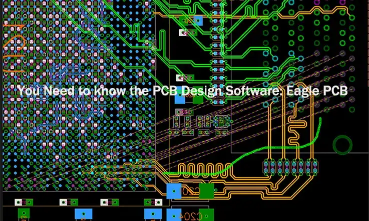
At JarnisTech, we are passionate about PCB design and believe that this skill is of great benefit to electronics enthusiasts of all levels. To this end, we have created a series of tutorials to teach you the fundamentals of Eagle PCB design.
Before delving into the specifics of Eagle PCB design, it is important to understand why this software is an excellent choice for your PCB design needs. Eagle offers a multitude of features and benefits that make it an indispensable tool for creating high-quality PCB designs. By utilizing Eagle, you can streamline your design process and produce reliable and efficient PCBs with ease.
We are excited to share our knowledge and expertise in Eagle PCB design with you, and look forward to helping you develop your skills in this important area of electronics engineering.
What Is Eagle PCB?
Eagle PCB (Printed Circuit Board) is a software tool used for designing and creating electronic circuit boards. It is a popular software package developed by Autodesk that allows users to create schematics and layouts for printed circuit boards.
Eagle PCB is commonly used by engineers, designers, and hobbyists for designing and prototyping electronic circuits. The software provides a user-friendly interface that includes a schematic editor, a PCB layout editor, and a library editor.
Using Eagle PCB, users can create and edit electronic circuits, add components, and connect them using wires and traces. The software also provides a wide range of features such as autorouting, design rule checking, and schematic capture.
Eagle PCB allows users to export their designs in various file formats, including Gerber files for manufacturing. It can also be integrated with other software tools such as SPICE simulation software and 3D CAD software to enhance the design process.
Getting Started with Eagle PCB
Here’s an overview of getting started with Eagle PCB:
1. Download and Install Eagle PCB: You’ll need to download and install the Eagle PCB software from the Autodesk website. Follow the installation instructions provided on the website to complete the installation process.
2. Launch Eagle PCB: Once you’ve installed Eagle PCB, launch the software by double-clicking on the application icon.
3. Create a New Project: In Eagle PCB, a project is a container for all the files related to a specific design. To create a new project, go to the File menu and select New > Project. Enter a name for your project and choose a location to save it.
4. Add Components to a Schematic: In Eagle PCB, you’ll start by creating a schematic of your design. To add components to your schematic, select the Add Part tool from the toolbar and click on the schematic editor where you want to place the component. You can also search for components in the Eagle PCB library and add them to your design.
5. Connect Components on a Schematic: To connect components on a schematic, use the Net tool to draw wires between the pins of your components. You can also use the Bus tool to connect multiple wires together.
6. Generate a Netlist: Once you’ve created your schematic, you’ll need to generate a netlist. This is a list of all the components in your design and how they’re connected. To generate a netlist, go to the File menu and select Export > Netlist. Choose a location to save your netlist file.
7. Create a Board Layout: With your netlist file, you’ll now create a board layout in Eagle PCB. Go to the File menu and select New > Board. Eagle PCB will import your netlist and create a board with all the components and connections from your schematic.
8. Place Components on a Board: In the board layout editor, you’ll need to place your components on the board. Use the Move tool to drag components into position.
9. Route Connections on a Board: With your components placed, you’ll need to route the connections on your board. Use the Route tool to draw traces between your components.
10. Generate Gerber Files: Once you’ve completed your board layout, you’ll need to generate Gerber files. These are the files used to manufacture your PCB. To generate Gerber files, go to the File menu and select CAM Processor. Choose a location to save your Gerber files and follow the instructions provided by Eagle PCB.
That’s a brief overview of getting started with Eagle PCB. There are many more features and tools available in the software, so it’s worth exploring the documentation and tutorials to get the most out of it.
How Does Eagle PCB Function?
Eagle PCB design software utilizes electronic design automation to enable circuit designers to perform multiple operations simultaneously. The software is designed using the model interface method, allowing for efficient and effective PCB design.
The software is composed of several key views, including the Control Panel, Library, Schematic, and Board Layout. The Control Panel serves as the primary window for controlling the various functions of the software and launching other windows.
The Eagle PCB library is a rich and versatile resource that provides a wide range of design tools to optimize the PCB design process. It allows designers to edit and regulate the functionalities of parts and components, ensuring that they meet the specific needs of the project.
The Schematic view is where designers place the PCB components and connect the pins to their designated segments. This view defines the parts and their connections, with components typically placed according to electrical considerations.
Finally, the Board Layout view is where designers place their project and connect it in accordance with the schematics. Here, parts are connected in a way that makes physical sense. The Board Layout view is critical in ensuring that the final PCB design is both functional and practical.
Why Choose the Eagle PCB Design Software?
Eagle PCB Design Software is a popular and highly-regarded PCB CAD software that offers a range of unique and beneficial features. Below are some of the reasons why Eagle PCB Design Software is an excellent choice for circuit designers:
User Interface: Eagle PCB has a highly customizable user interface that allows users to create custom toolbars, hotkeys, and scripts. This makes it easier for users to work efficiently and customize the software to their needs.
Library Parts: Eagle PCB has a large library of components and footprints that users can use in their designs. The library is continually updated with new parts and is maintained by the software developer, Autodesk. In addition, users can create their own custom library parts.
Lightweight: Eagle requires a minimal amount of disk space ranging from 50 to 200 MB, as compared to other advanced tools that may require over 10 GB. Its installer is also compact, at approximately 25 MB, allowing for quick and easy installation within minutes.
Cross-Platform: Eagle is a cross-platform software that can run seamlessly on Linux, Mac, and Windows, making it highly versatile and accessible to designers across multiple operating systems.
Community Support: Eagle enjoys a strong and supportive community of PCB designers who appreciate its functionality and user-friendly interface. This community means that designers can easily access a wealth of knowledge and resources, including pre-existing designs of popular components and circuit boards.
Simulation: Eagle PCB has a built-in simulation tool called SPICE that allows users to simulate the behavior of their circuits before building them. This can help users identify potential problems and optimize their designs.
3D Modeling: Eagle PCB has a built-in 3D modeling tool that allows users to visualize their designs in 3D. This can help users check for mechanical interference and visualize how their components will fit together.
Collaboration: Eagle PCB doesn’t have built-in collaboration tools, which can make it difficult to collaborate on designs with others. However, it does support exporting designs in various formats, which can be shared with others who use different PCB design software.
Low or Free Cost: Eagle offers a freeware version that provides sufficient utility for designing most printed circuit boards. However, for those who need more advanced features, upgrading to a higher plan is relatively inexpensive compared to other high-end tools, making it an affordable option for both hobbyists and professionals.
Overall, Eagle PCB Design Software is an excellent choice for designers looking for a lightweight, cross-platform, cost-effective solution that is backed by a supportive community.
What Are The Limitations Of Eagle PCB?
As with any software, Eagle PCB has its limitations. Here are some of the most common limitations of Eagle PCB:
Limited Free Version: The free version of Eagle PCB has some limitations, such as a limited board size and limited number of schematic sheets. If you need to create larger or more complex designs, you’ll need to purchase a license for the full version.
Limited Library Parts: While Eagle PCB has a large library of components and footprints, it may not have every component you need. You may need to create your own custom parts or search for third-party libraries.
Limited Routing Options: Eagle PCB has a limited set of routing options, which may not be sufficient for complex designs. You may need to manually route connections or use a third-party routing tool.
Limited 3D Modeling: While Eagle PCB has a built-in 3D modeling tool, it’s not as advanced as some other 3D modeling tools. You may need to use a separate 3D modeling tool to create more complex 3D models.
Limited Simulation Options: While Eagle PCB has a built-in simulation tool called SPICE, it’s not as advanced as some other simulation tools. You may need to use a separate simulation tool to simulate more complex circuits.
Steep Learning Curve: Eagle PCB has a steep learning curve, especially for beginners. It can take some time to learn how to use all of the features and tools in the software.
Limited Collaboration Options: Eagle PCB doesn’t have built-in collaboration tools, which can make it difficult to collaborate on designs with others. You may need to use a separate collaboration tool or share files manually.
These are some of the most common limitations of Eagle PCB. However, despite its limitations, Eagle PCB is still a popular and powerful PCB design tool used by many professionals and hobbyists.
How to Check The Design Rules In Eagle PCB?
Design rules are a crucial aspect of Eagle PCB design as they ensure that schematics are error-free and that the end product is of high quality. The design rule checks (DRCs) in Eagle software play a vital role in ensuring that design rules are adhered to and that any errors are identified.
When accessing the DRC dialog box in Eagle software, there are several tabs that you can navigate to set and check your design rules. These tabs include:
File: This section contains downloadable .drc files that can be used to check the design rules.
Layers: Depending on your version of Eagle, you may be able to check the designs of multiple layers.
Clearance: This tab allows you to set the minimum distance between different components used on the circuit board design.
Distance: Here, you can set the drill hole diameter, copper trace thickness, and other relevant dimensions.
Sizes: You can set the minimum size of drill bits and different micro and blind PCB vias.
Restring: This tab controls the dimensions of through-hole vias.
Shapes: Here, you can set the design rules for PCB pads with round edges.
Supply: This tab controls the dimensions of thermal vias used in the PCB traces.
Masks: This tab controls the use of masks on required positions of the PCB.
Misc: Here, you can check various parameters such as the grid, angle, restrict, font, etc.
Once you have completed the required tabs, you can start checking your design. One benefit of using Eagle PCB Design Software is that designers do not need to interfere with the design while checking it. Additionally, Eagle PCB crack can be utilized to further aid the design process. However, it is important to note that using cracked versions of software is illegal and can lead to various issues, including security risks and legal consequences.
Conclusion
Eagle PCB is a powerful and popular PCB design software that has many features and capabilities. It has a highly customizable user interface, a large library of components and footprints, a built-in simulation tool, and a 3D modeling tool. While it has some limitations, such as a limited free version and limited collaboration options, it’s still a popular choice for hobbyists and small projects. Choosing the right PCB design software ultimately depends on the user’s needs, preferences, and budget, but Eagle PCB is definitely worth considering for those looking for a powerful and affordable PCB design tool.
In a word, Eagle PCB is a highly regarded software that promotes the manufacturing quality of printed circuit boards, thanks to its numerous outstanding features and user-friendly interface. It has become a popular circuit solution for designers in the present day.
At JarnisTech, we specialize in researching, manufacturing, developing, and supplying Eagle PCBs with unmatched reliability. We are committed to providing comprehensive information about PCB design through this FAQ guide and are available to assist with any PCB-related issues you may encounter. Stay connected with us for updates and the latest developments in PCB design.
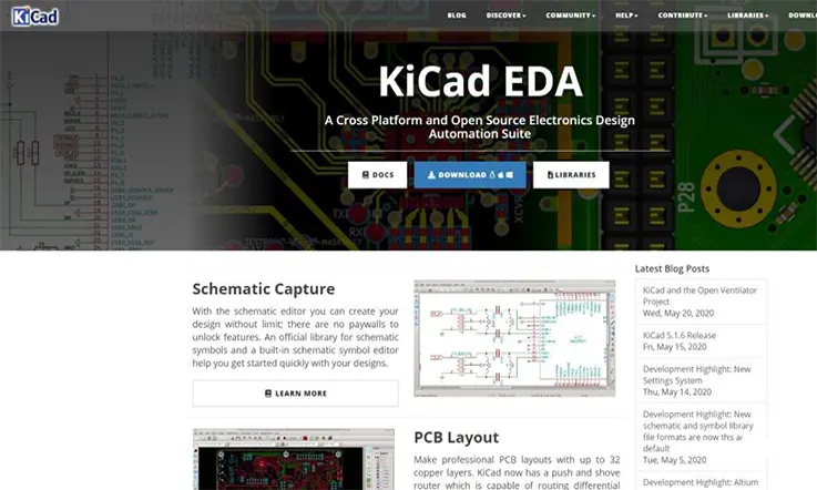
JarnisTech is a renowned Kicad PCB manufacturing company, serving customers in over 60 countries around the globe. We specialize in the production of high-quality Kicad PCBs, leveraging our expertise in utilizing the Kicad software to design and meet the specific requirements of our clients. Our dedication lies in delivering efficient, functional, and durable PCBs that excel in terms of quality.
This comprehensive FAQ guide is designed to enhance your knowledge about Kicad PCBs. It contains valuable information that will provide you with a thorough understanding of this popular type of printed circuit board. If you are interested in expanding your knowledge, we encourage you to read through the entirety of this guide.
What Is a Kicad ?
KiCAD is a widely used open-source software that facilitates the design of electronic schematics and the subsequent transfer of these schematics to a PCB layout. One notable advantage of KiCAD is that it generates text files, which offer a straightforward approach for manual modification or the development of custom scripts. Moreover, KiCAD is a versatile software that supports multiple platforms including Microsoft Windows, OS X, and Linux.
Beneath its user-friendly interface, KiCAD comprises a collection of standalone software tools, meticulously integrated to form a cohesive system. These tools work harmoniously to provide an elegant and efficient solution for electronic design tasks.
Program Name
Description
File Extension
KiCAD
Project manager
*.pro
Eschema
Schematic editor (both schematic and component)
*.sch, *.lib, *.net
CvPcb
Footprint selector
*.net
Pcbnew
Circuit board editor
*.kicad_pcb
Gerb View
Gerber viewer
All the usual Gerber
Bitmap2component
Convert bitmap images to components or footprints
*.lib, *.kicad_mod, *.kicad_wks
PCB Calculator
Calculator for components, track width, electrical spacing, color codes, and more
None
Pl Editor
Page layout editor
*.kicad_wks
KiCad has gained significant maturity and reliability, making it an excellent choice for the successful development and ongoing maintenance of intricate electronic boards. Notably, KiCad surpasses any limitations related to board size, allowing seamless handling of complex designs. With the capacity to accommodate up to 32 copper layers, 14 technical layers, and 4 auxiliary layers, KiCad offers exceptional versatility.
One of KiCad’s strengths lies in its ability to generate comprehensive sets of files essential for the fabrication of printed circuit boards. These include Gerber files for photo-plotters, drilling files, component location files, and various other formats needed in the production process. As an open-source software licensed under GPL, KiCad becomes an optimal tool for projects aimed at fostering the development of electronic hardware with an open-source ethos.
Kicad PCB Definition
Kicad is a software utilized for Electronic Design Automation (EDA), specifically renowned for its capability to facilitate the design process of printed circuit boards (PCBs). With Kicad, users can seamlessly transition from schematic design to PCB layout.
Kicad provides a comprehensive and well-rounded environment for both schematic design and layout design stages. It empowers designers to create schematics with ease and precision. Furthermore, Kicad offers a range of features including generating a materials list, producing Gerber files, generating artwork, providing 3D views of the PCB, and component integration within the Kicad PCB environment. These features contribute to a holistic design experience, ensuring accurate and efficient realization of the circuit board design.
What Are The Features Of Kicad PCB?
This software possesses distinct attributes that set it apart. The PCB undergoes a meticulous design process, ensuring a harmonious environment throughout each step. This process encompasses crucial stages such as PCB layout, schematic design, library editing, and Gerber file generation, all meticulously executed.
Some of the features of KiCad PCB include:
Schematic Capture: KiCad allows users to create and edit electronic schematics using a graphical interface.
PCB Layout: KiCad provides a powerful PCB layout editor that allows users to place components, route traces, and create custom footprints.
3D Viewer: KiCad has an integrated 3D viewer that allows users to view their PCB designs in 3D and check for any mechanical conflicts.
Design Rule Checking (DRC): KiCad includes a DRC tool that checks for design rule violations, such as minimum trace width and clearance, before sending the design for manufacturing.
Gerber/Excellon file generation: KiCad can generate Gerber and Excellon files required for manufacturing the PCB.
Library Management: KiCad has a built-in library management system that allows users to create and manage their own custom component libraries.
Multi-platform support: KiCad is available for Windows, Linux, and Mac OS, making it accessible to a wide range of users.
Community support: KiCad has a large and active community of users who contribute to its development, provide support and guidance to new users, and share their knowledge and resources.
The utilization of cross-platform software, programmed in C++, is a prominent characteristic of this system. A notable advantage is the ability to incorporate personalized components into your Kicad PCB. These custom components can be project-specific or installed for broader application.
Furthermore, Kicad PCB supports the utilization of third-party libraries, which offer additional component options. Notably, the configuration files are thoughtfully structured in plain text format, ensuring easy organization. Moreover, this software facilitates seamless integration with version control systems and enables the automation of component generation through scripting capabilities.
How Does kicard PCB work?
KiCad PCB works by allowing users to create a schematic diagram of their electronic circuit and then converting it into a physical layout for a printed circuit board (PCB). Here’s a general overview of how KiCad PCB works:
Schematic Capture: The first step is to create a schematic diagram of the electronic circuit using KiCad’s schematic editor. This involves selecting the components needed for the circuit and connecting them together using wires or buses. KiCad provides a wide range of built-in components, and users can also create their own custom components if needed.
Netlist Generation: Once the schematic is complete, KiCad generates a netlist, which is a list of all the connections between the components in the circuit. The netlist is used to create the physical layout of the PCB.
PCB Layout: The netlist is imported into KiCad’s PCB layout editor, where the components are placed onto the physical layout of the PCB and connected with traces and vias. The PCB layout editor allows users to customize the layout and routing of the PCB, including the placement of components, the routing of traces, and the creation of custom footprints for components.
Design Rule Checking (DRC): After completing the PCB layout, KiCad’s DRC tool is used to check for any design rule violations, such as minimum trace width and clearance. This helps ensure that the design is manufacturable and meets the specifications of the user’s chosen PCB manufacturer.
Gerber/Excellon File Generation: Once the PCB design has passed DRC, KiCad can generate Gerber and Excellon files that describe the layout of the PCB. These files are used by PCB manufacturers to create the physical board.
Overall, KiCad PCB works by providing a suite of tools for creating and designing electronic circuits, generating netlists and physical layouts, and checking the design for manufacturability. It is a powerful and versatile tool that is widely used by hobbyists, students, and professionals alike.
Getting Started with KiCad PCB
1. Download and install KiCad PCB: You can download the latest version of KiCad PCB from the official website. The installation process is generally straightforward and involves accepting the license agreement and selecting the components you want to install.
2. Create a new project: Once you’ve installed KiCad PCB, you can create a new project by clicking “File” > “New Project” and selecting “New Project” from the dropdown menu. You’ll then be prompted to give your project a name and select a location to save it.
3. Create a schematic: The first step in designing a PCB is to create a schematic. To do this, click “File” > “New” > “Schematic” and start adding components to your schematic. You can access the component libraries by clicking “Place” > “Component” and selecting the library you want to use.
4. Connect components: Once you’ve added all the components to your schematic, you can connect them by adding wires. To do this, click “Place” > “Wire” and click on the pins you want to connect. You can also add labels to your schematic by clicking “Place” > “Label”.
5. Create a PCB layout: Once you’ve completed your schematic, you can create a PCB layout from it. To do this, click “Tools” > “Annotate Schematic” to assign footprints to your components, and then click “Tools” > “Update PCB from Schematic” to create the PCB layout.
6. Place components: Once you’ve generated the PCB layout, you can start placing components on it. To do this, click “Place” > “Footprint” and select the component you want to place. You can then drag the component to the desired location on the board.
7. Route traces: Once you’ve placed all the components, you can start routing the traces that connect them. To do this, click “Route” > “Interactive Router” and start clicking on the start and end points of the traces you want to create. KiCad PCB will automatically generate curved traces that follow the path of least resistance.
8. Export your design: Once you’ve completed your PCB design, you can export it to the appropriate file formats for manufacturing. To do this, click “File” > “Plot” and select the output format you want to use, such as Gerber files or a Bill of Materials (BOM).
Tips and Tricks for Using KiCad PCB
Here are some tips and tricks for using KiCad PCB:
Keyboard shortcuts: KiCad PCB has a number of useful keyboard shortcuts that can save you time and effort. For example, pressing “E” in the schematic editor will open the properties dialog for a selected component, while pressing “M” in the PCB layout editor will switch to the move tool.
Interactive router: The interactive router is a powerful tool that can save you a lot of time when routing traces on your PCB. It allows you to route traces by clicking on the start and end points, and automatically generates curved traces that follow the path of least resistance.
Custom footprints: If you can’t find a footprint for a particular component in KiCad PCB’s built-in libraries, you can create your own custom footprint using the Footprint Editor. This can be a bit time-consuming, but it’s worth it if you’re using a component that’s not widely available.
Importing and exporting files: KiCad PCB supports a wide range of file formats, so you can easily import and export files to and from other PCB design software. For example, you can import Eagle CAD files or export your KiCad PCB design to Gerber files for manufacturing.
Libraries: KiCad PCB has a number of built-in libraries for common components, but you can also download and add custom libraries if you need to use specific components that aren’t included in the default libraries.
Design rule checker: The Design Rule Checker is a tool that can help you ensure that your PCB design meets certain standards and guidelines, such as minimum trace width and clearance. It can save you a lot of time and effort in the long run by catching potential issues early on.
Why Use KiCad for Your PCB Design ?
KiCad provides numerous advantages for printed circuit board design, including:
Open-source: KiCad operates as an open-source PCB design platform, fostering a collaborative environment among developers and enabling partnerships. Users can engage with a global community of PCB manufacturers and designers.
Free of Charge: KiCad does not require any payment or subscription for its download and usage. However, users have the option to support the software through voluntary donations.
Cross-platform Compatibility: This PCB design software is compatible with MacOS, Linux, and Windows. Project files created on one operating system can seamlessly transfer to another, ensuring flexibility and convenience.
Open Part Libraries: KiCad offers publicly accessible component libraries that encompass comprehensive collections of schematic symbols, 3D models, and footprints. Contributors continually develop and expand the library, providing a wide variety of resources. Users can effortlessly download and incorporate these components into their designs, and they can also contribute their own footprints and symbols to the library.
Reliable and Extensible: With its predominantly C/C++ programming, KiCad delivers exceptional performance across different systems. Moreover, KiCad leverages the capabilities of users’ graphics cards to enhance the display of graphical elements. The software supports Python scripting, allowing users to extend its features and streamline workflows effectively.
What Are The Disadvantages Of Kicad PCB?
While KiCad PCB is a popular and widely used PCB design tool, there are some potential disadvantages to consider:
Steep learning curve: KiCad PCB has a steep learning curve, especially for beginners who are new to PCB design. It can take some time to get familiar with the software and its various tools and features.
Limited community support: While KiCad PCB has a dedicated community of users and contributors, it may not have the same level of support and resources as some other PCB design tools. This can make it more difficult to find answers to specific questions or issues.
Limited 3D modeling capabilities: KiCad PCB’s 3D modeling capabilities are somewhat limited compared to some other PCB design tools. While it does have a 3D viewer, it may not be as advanced or flexible as other software options.
Limited collaboration features: KiCad PCB does not offer advanced collaboration features, such as real-time collaboration or version control. While it is possible to collaborate on projects using external tools, this can be more difficult and time-consuming.
Lack of built-in simulation tools: KiCad PCB does not have built-in simulation tools, which can make it more difficult to simulate and test your designs before manufacturing. However, there are external simulation tools that can be used in conjunction with KiCad PCB.
It’s worth noting that many of these potential disadvantages can be mitigated with experience and familiarity with the software, as well as by using external tools or resources to supplement KiCad PCB’s capabilities.
Future Developments and Potential Improvements
KiCad PCB has been steadily improving over the years, and there are several future developments and potential improvements on the horizon. Here are a few examples:
Improved user interface: KiCad PCB has undergone several UI updates in recent years, but there is still room for improvement. Future updates could include more intuitive and user-friendly interfaces, improved workflow, and customizable toolbars.
Improved 3D modeling: While KiCad PCB has a 3D viewer, there is potential for further development in this area. This could include more advanced 3D modeling capabilities, such as the ability to create and manipulate 3D models directly within the software.
Integration with cloud-based services: Cloud-based services are becoming increasingly popular in the PCB design and manufacturing industry. Future developments could include integration with cloud-based services, such as collaborative design platforms and cloud-based simulation tools.
Improved collaboration features: While KiCad PCB does offer some collaboration features, such as the ability to export and import designs from other software tools, there is potential for further development in this area. This could include real-time collaboration features, version control, and commenting and markup tools.
Improved simulation and analysis capabilities: While KiCad PCB does not have built-in simulation tools, there is potential for integration with external simulation and analysis tools. Future developments could include closer integration with simulation tools and more advanced simulation capabilities directly within the software.
As a result, there is significant potential for future developments and improvements in KiCad PCB, and these developments could help to further improve the software’s capabilities and make it even more valuable for PCB designers and manufacturers.
Final Thoughts
KiCad PCB is a robust and versatile software solution for PCB design, offering an array of features and capabilities that cater to the needs of both designers and manufacturers. While beginners may encounter a learning curve, once acquainted with its tools and functionalities, the software proves user-friendly.
KiCad stands out as an invaluable design software for printed circuit board professionals. Unlike other alternatives in the market, it offers the advantage of being freely accessible, enabling users to create their PCB designs in accordance with the processes outlined in the article. Additionally, for more intricate PCB designs, seeking assistance from experienced professionals, particularly for hobbyist designers, can be a prudent choice. Furthermore, companies like JarnisTech PCB & Assembly can provide comprehensive solutions to meet various PCB requirements.
In conclusion, KiCad PCB is a highly commendable choice for those seeking a powerful and versatile PCB design software that combines accessibility, customization, and a broad range of features and capabilities. Its usage can unlock significant potential in your design endeavors.
Altium and Eagle are two of the most popular electronic design automation (EDA) software tools used in the industry for designing printed circuit boards (PCBs). Both Altium and Eagle provide users with a range of features for schematic capture, PCB layout, and design rule checking, among others. However, there are some differences in the capabilities and user experience of these two tools that make them better suited to different types of users and projects. In this article, we will explore the main differences between Altium and Eagle and help readers determine which tool is best suited to their specific needs.
What Is Eagle PCB?
EAGLE (Easily Applicable Graphical Layout Editor) is a flexible and powerful electronics design automation (EDA) application that includes schematic capture, printed circuit board (PCB) layout, and auto-router tools.
EAGLE is a popular choice among many hobbyists, makers, and professionals for designing and laying out PCBs because of its relatively low learning curve, affordability, and wide acceptance in the community. As of my knowledge cut-off in September 2021, EAGLE is owned by Autodesk, a company well known for their powerful design and engineering software tools.
Key Features of EAGLE PCB:
Schematic Editor: This allows you to design your circuits with various components and then connect these components to form a complete circuit design.
PCB Layout Editor: Once the schematic design is complete, EAGLE can generate a board layout where you can place and route the components.
Auto-router: The auto-router feature can automatically route your traces for you based on a set of rules you specify, a useful feature for complex designs.
Library: EAGLE has a vast library of components to choose from when designing your schematic and board.
EAGLE supports various file formats for the output of your design, allowing you to create Gerber files, which are the industry standard for PCB manufacture.
Remember, while EAGLE has many powerful features, like any tool, it has limitations and may not be the best tool for every job.
What Is Altium PCB?
Altium PCB (Printed Circuit Board) is a software tool suite designed for electronic design automation (EDA) and PCB design. Altium PCB is developed by Altium Limited, an Australian software company specializing in PCB design software and other electronic design solutions.
Altium PCB provides a comprehensive set of features and functionalities to facilitate the design, layout, and manufacturing of printed circuit boards. It offers a user-friendly interface coupled with advanced design capabilities, making it a popular choice among engineers and PCB designers.
Key Features of Altium PCB Include:
Schematic Capture: Altium PCB allows users to create and edit schematic diagrams, defining the electrical connections and components of the circuit.
PCB Layout: It provides tools for creating the physical layout of the PCB, including placing components, routing the traces, and defining the board outline.
3D Visualization: Altium PCB offers a 3D design environment that allows users to visualize their PCB in three dimensions, enabling better design analysis and verification.
Design Rule Checking (DRC): DRC ensures that the PCB design adheres to specific manufacturing and electrical constraints, helping to identify and resolve potential issues.
Signal Integrity Analysis: Altium PCB includes simulation and analysis tools to assess signal integrity, identifying potential problems like impedance mismatches or high-speed signal degradation.
Library Management: The software provides a library management system to store and organize component libraries, enabling easy access to commonly used parts.
Collaboration and Documentation: Altium PCB supports collaborative design workflows, allowing multiple designers to work on the same project simultaneously. It also includes documentation tools for generating manufacturing files, assembly drawings, and other documentation required for PCB fabrication.
Altium PCB is widely used in various industries, including consumer electronics, aerospace, automotive, telecommunications, and industrial automation, among others. It helps engineers and designers
What Is the Difference Between Altium and Eagle ?
Altium and Eagle are both popular software tools used for electronic design automation (EDA), specifically for printed circuit board (PCB) design. While they share similarities in their purpose, there are several differences between Altium and Eagle. Here are some key distinctions:
Key Similarities and Differences between Altium and Eagle
Altium and Eagle have many similarities, such as providing users with a wide range of features for PCB design. However, there are also some key differences that set them apart. Here are some of the main similarities and differences between Altium and Eagle:
Similarities:
● Both Altium and Eagle offer schematic capture and PCB layout tools.
● Both tools provide users with design rule checking and error reporting features.
● Both offer 3D visualization of PCB designs.
● Both have extensive component libraries and a range of customization options.
Differences:
● Altium is generally considered to be more powerful, feature-rich and scalable than Eagle, making it more suitable for complex designs and large-scale projects.
● Eagle is generally considered to be more accessible and easier to use for beginners and small-scale projects.
● Altium offers advanced features such as multi-board design, FPGA design, and signal integrity analysis, which are not available in Eagle.
● Altium also has a more extensive range of design rule checks and can handle more complex design rules.
● Eagle has a more affordable pricing structure and a free version with limited features, making it more accessible to hobbyists and small businesses.
● Altium has a steeper learning curve and requires more training and experience to use effectively, while Eagle is more intuitive and user-friendly.
Overall, the choice between Altium and Eagle will depend on the user’s specific needs, budget, and level of expertise.
Design Capabilities and Features Comparison
Altium and Eagle offer a range of design capabilities and features that are essential for PCB design. Here is a comparison of some of the key design capabilities and features of Altium and Eagle:
Design Capabilities:
● Altium offers advanced capabilities such as multi-board design, FPGA design, and signal integrity analysis, which are not available in Eagle.
● Eagle is generally considered more suitable for small-scale designs and simpler projects, while Altium is more suited for larger and more complex designs.
Schematic Capture:
● Both Altium and Eagle offer schematic capture tools that allow users to design and edit schematic diagrams.
● Altium has a more powerful schematic capture tool with advanced features such as hierarchical schematics and design reuse, while Eagle offers a simpler and more straightforward schematic capture tool.
PCB Layout:
● Both Altium and Eagle offer PCB layout tools that allow users to design and edit PCB layouts.
● Altium has a more robust and feature-rich PCB layout tool, with advanced features such as differential pair routing, interactive routing, and copper pour management.
● Eagle offers a more straightforward and intuitive PCB layout tool with fewer advanced features, making it easier for beginners to use.
Design Rule Checking:
● Both Altium and Eagle offer design rule checking tools that detect design errors and inconsistencies.
● Altium has a more extensive range of design rule checks and can handle more complex design rules, making it more suitable for advanced designs.
● Eagle offers a simpler and more straightforward set of design rule checks, which is more suitable for simpler designs.
3D Visualization:
● Both Altium and Eagle offer 3D visualization of PCB designs, allowing users to visualize their designs in a realistic 3D environment.
● Altium’s 3D visualization tool is more powerful and versatile and allows users to create complex 3D models of their designs.
● Eagle’s 3D visualization tool is more basic and is mainly used for basic visualizations of PCB designs.
So, Altium offers more advanced and powerful design capabilities and features, while Eagle offers a more accessible and user-friendly design environment. The choice between Altium and Eagle will depend on the user’s specific needs and level of expertise.
Ease of Use and Learning Curve Comparison
Altium and Eagle both have different levels of ease of use and learning curves. Here is a comparison of their ease of use and learning curves:
Ease of Use:
● Eagle is generally considered to be more accessible and user-friendly than Altium. It has a simpler and more intuitive user interface, making it easier for beginners to get started.
● Altium, on the other hand, has a steeper learning curve due to its advanced features and capabilities. It requires more training and experience to use effectively.
Learning Curve:
● Eagle has a shorter learning curve than Altium since it is easier to use and has fewer advanced features. Users can learn the basic functions of Eagle in a relatively short amount of time.
● Altium, on the other hand, has a longer learning curve due to its advanced features and capabilities. Users require more training and experience to master Altium’s advanced functions and capabilities.
Documentation and Support:
● Both Eagle and Altium have extensive documentation and support resources to help users learn and use the software effectively.
● Eagle has a large and active community of users who can provide support and advice, making it easy for beginners to get help.
● Altium offers extensive documentation and training resources, including online courses and user guides, making it easier for users to learn and master the software.
As a result, Eagle is more suitable for beginners and users with less experience due to its user-friendly interface and shorter learning curve. Altium is more suitable for advanced users and professionals who require more advanced features and capabilities and are willing to invest more time and effort into learning the software.
Pricing and Licensing Comparison
Altium and Eagle have different pricing models and licensing options. Here is a comparison of their pricing and licensing:
Pricing:
● Altium is a more expensive software than Eagle, with a higher upfront cost and yearly subscription fees. The cost of Altium varies depending on the version and the level of functionality required.
● Eagle has a more affordable pricing structure, with a free version with limited features and paid versions that range from affordable to moderately expensive. The cost of Eagle varies depending on the version and the level of functionality required.
Licensing:
● Altium uses a subscription-based licensing model, which requires users to pay a yearly fee to access the software and receive updates and support. Altium also offers a perpetual licensing option that allows users to own the software outright.
● Eagle uses a perpetual licensing model, which allows users to own the software outright. Users can purchase a license for a specific version of the software and receive updates and support for a limited time. After that time, users can choose to renew their license or continue using the software without updates and support.
Overall, Eagle has a more affordable pricing structure, making it accessible to hobbyists and small businesses. Altium is more suitable for larger corporations and professional users who require more advanced features and capabilities. The choice between Altium and Eagle will depend on the user’s specific needs and budget.
Community Support Comparison
Community support is an important factor to consider when choosing between Altium and Eagle. Here is a comparison of their community support:
Altium Community Support:
● Altium has an active and supportive community of users who share knowledge, tips, and advice on using the software.
● Altium provides users with access to a range of resources, including online forums, user groups, and blogs, where users can ask questions and get help.
● Altium also offers extensive documentation and training resources, including online courses and user guides, making it easier for users to learn and master the software.
Eagle Community Support:
● Eagle also has an active community of users who provide support and advice to other users.
● Eagle’s community support is largely based on online forums and user groups, where users can ask questions and share knowledge.
● Eagle also provides users with extensive documentation and training resources to help users learn and use the software effectively.
Overall, both Altium and Eagle have active and supportive communities that provide users with access to a range of resources and support. Altium’s community support is more extensive, with a wider range of resources and training options. However, Eagle’s community support is still robust and can provide users with the help and advice they need to use the software effectively.
Conclusion and Recommendations Based on Specific User Needs
Altium and Eagle are both powerful EDA software tools that offer a range of features and capabilities for PCB design. The choice between Altium and Eagle depends on the user’s specific needs, budget, and level of expertise.
For users who require advanced features and capabilities, Altium is the better choice. Altium offers advanced capabilities such as multi-board design, FPGA design, and signal integrity analysis, which are not available in Eagle. Altium also has a more extensive range of design rule checks and can handle more complex design rules, making it more suitable for advanced designs. However, Altium is more expensive and has a steeper learning curve, making it more suitable for professional users and larger corporations.
For users who require an accessible and user-friendly PCB design tool, Eagle is the better choice. Eagle has a simpler and more intuitive user interface, making it easier for beginners to get started. Eagle is also more affordable than Altium, with a free version with limited features and paid versions that range from affordable to moderately expensive. However, Eagle is not as powerful as Altium and may not be suitable for more complex or advanced designs.
Ultimately, the choice between Altium and Eagle depends on the user’s specific needs and requirements. Users should consider their design requirements, budget, and level of expertise when choosing between these two software tools. It may also be helpful to try both tools and compare their features and capabilities before making a final decision.
Backplane PCBs are crucial connector printed circuit boards used in various applications, projects, and products, making them increasingly valuable in modern times. They offer greater functionality and benefits for PCB fabrication.
JarnisTech is a leading manufacturer that specializes in backplane PCBs. Given the significant importance of these PCBs in fabrication, JarnisTech employs a meticulous manufacturing process and utilizes state-of-the-art technologies.
Whether you seek specific information about this particular type of printed circuit board or are interested in gaining insights into our backplane PCB facilities, this comprehensive guide will provide you with all the necessary details. It covers a wide range of topics related to backplane PCBs, ensuring you are well-informed about their capabilities and advancements.
What is a Backplane PCB ?
A backplane PCB serves as a vital component in electronic systems as it facilitates the interconnection of multiple devices. Acting as the central interface, it forms the backbone that enables seamless communication and data transfer among various subsystems and components.
Essentially, a backplane PCB comprises an array of connectors, slots, and sockets that facilitate the insertion of diverse modules or daughter cards. These modules encompass a wide range of devices, such as CPUs, memory modules, input/output cards, and more. Through the backplane, these modules establish power and data connections, fostering efficient communication and data exchange among them.
Design Considerations for Backplane PCBs
Designing a backplane PCB involves several considerations to ensure its optimal performance. Some of the key design considerations for backplane PCBs are:
Layer count: The number of layers required for a backplane PCB depends on the complexity of the system and the number of signals to be routed. A higher number of layers can provide better signal integrity, but also increase the cost and complexity of fabrication.
Trace width and spacing: The trace width and spacing must be carefully designed to ensure that the backplane can handle the required current and provide a low impedance path for signals. The trace width and spacing must be optimized for the specific signal frequency, skew, and crosstalk requirements.
Materials selection: Backplane PCBs are typically made using high-performance materials that provide good electrical properties, such as FR-4, polyimide, and Rogers materials. The selection of materials depends on the specific requirements of the system, such as thermal management, mechanical strength, and electrical performance.
Thermal management: Backplane PCBs can generate a significant amount of heat, especially in high-performance systems. Adequate thermal management must be incorporated into the design to ensure that the backplane can operate within the required temperature range. This can include the use of thermal vias, embedded heat sinks, and proper component placement.
Signal integrity: Backplane PCBs must maintain signal integrity to ensure reliable communication between components. This requires careful consideration of trace length, impedance matching, and termination techniques.
Electrical performance: Backplane PCBs must meet the electrical performance requirements of the system, such as voltage, current, and power requirements. This requires careful consideration of the design parameters and simulation of the electrical performance using software tools.
EMI/EMC: Backplane PCBs must also consider electromagnetic interference (EMI) and electromagnetic compatibility (EMC) requirements to avoid interference with other components and systems. This requires careful shielding and grounding techniques, as well as compliance with regulatory standards.
Overall, the design of a backplane PCB requires careful consideration of multiple factors to ensure optimal performance and reliability.
Types of Backplane PCB
Backplane PCBs incorporate printed circuit boards featuring expansion slots or sockets to facilitate interconnection with other printed circuit boards. There exist two primary types of backplane PCBs: active backplanes and passive backplanes. Both variants effectively cater to industrial requirements.
Active Backplane PCB
An active backplane PCB incorporates motherboard circuitry and bus control for facilitating communication among its slots. It features the necessary slots and circuitry to maintain efficient data exchange on the board. Notably, an active backplane does not include processor complex components such as the central processing unit (CPU), cache, or chipset.
Passive Backplane PCB
A passive backplane PCB is equipped with circuitry designed for bus connections. It may incorporate drivers and buses depending on specific requirements. Essentially, a passive backplane primarily consists of bus connectors with minimal or no additional circuitry. The communication between boards is managed by expansion boards connected to the passive backplane. A passive backplane PCB can accommodate one or more expansion boards. In industrial settings, passive backplanes often feature bridges that establish connections between two buses, which can be of the same or different types.
How Does A Backplane PCB Work?
A Backplane PCB functions as a collection of electric connectors arranged in a parallel configuration. Each pin of every connector is connected to a common pin, effectively establishing connectivity across all pins.
Primarily, a Backplane PCB serves as a specialized form of PCB that provides structural support for connecting additional printed circuit boards. It enhances stability and mechanical strength in the PCB assembly.
Moreover, it serves as a platform for integrating daughterboards, which are additional components of the system.
Various daughterboards fulfill distinct functions within the PCB system. Backplane PCBs are highly versatile and widely employed, primarily due to their ability to facilitate the easy interchangeability of different cards.
Notably, backplane PCBs offer modularity, scalability, and other advantages that contribute to their suitability for diverse applications. When an external server signal enters the system, it passes through a daughter card and subsequently reaches the backplane PCB, which regulates the signal according to the required output.
Backplane Manufacturing Difficulties
Backplane manufacturing difficulties can arise due to various reasons. Backplanes are an essential component of electronic systems that provide a communication channel between different modules and components. These difficulties can arise during the design, fabrication, assembly, or testing stages. Some of the common backplane manufacturing difficulties are:
Signal Integrity Issues
One of the major difficulties in backplane manufacturing is ensuring signal integrity. Signal integrity issues can arise due to crosstalk, electromagnetic interference (EMI), and signal attenuation. These issues can result in signal distortion, data errors, and system failures.
Fabrication Issues
Backplane fabrication involves complex processes such as drilling, plating, and laminating. Any errors or defects during the fabrication process can result in signal loss, short-circuits, or open-circuits. Fabrication issues can also arise due to poor quality control, lack of precision, or improper tooling.
PCB Thickness: The increased thickness of Backplane PCBs is a result of incorporating numerous high-speed controlled impedance transmission lines, supply rail planes, and return paths. When transmitting high-frequency data over extended traces, wider signal traces are necessary to mitigate signal attenuations. To maintain impedance and minimize signal absorption, a thicker dielectric is required. However, augmenting trace width reduces signal density in a given layer’s unit area, while increasing the dielectric thickness contributes to an overall increase in PCB thickness.
As the number of signal layers, power planes, and return planes increases in pursuit of optimal performance, the layer count of the PCB can reach 20 or more. This presents a challenge for manufacturers in maintaining standard PCB thickness given the available materials and impedance matching parameters.
For backplanes up to a thickness of 5 to 6mm, high-speed fine PCB drilling for vias and connectors functions adequately. However, thicker PCBs necessitate larger drill diameters. Manufacturers are constrained by higher drill aspect ratios, such as 8:1, which can impede volumetric production. As a result, thicker PCBs require multiple drill passes for a single via.
PCB Pressing: In the manufacturing process of thicker backplanes, the complexity of drilling increases. Lengthy drill holes necessitate multiple drilling operations, resulting in reduced drilling accuracy and a decrease in PCB yield percentage. Moreover, the high frequency performance of the backplanes is compromised as a consequence.
High density etching: In a backplane PCB, the extensive number of connectors results in a substantial utilization of PCB real estate for mounting holes and pads. PCB designers face the challenge of increasing the density of signal routing while adhering to impedance and trace length requirements, instead of simply adding more layers to the PCB. This heightened signal density brings about increased complexity during etching, pushing the geometries of traces, via-holes, pad-holes, and annular rings towards the limits of fabrication tolerances.
Impedance matching: Achieving impedance matched PCB fabrication poses challenges when dealing with high-speed data transmissions on backplanes. It is generally not advisable to transmit data in the gigabits-per-second range over standard FR-4 materials. The selection of materials for backplane PCBs is influenced by factors such as dielectric constant and dissipation factor. This presents a challenge for PCB manufacturers, as they need to provide PCBs using the required materials. Additionally, ensuring transmission line impedance, via impedance, and connector pad-to-pin impedance further adds to the complexity. Introducing a new material type necessitates slight adjustments to the PCB manufacturing process at the manufacturer’s facility.
Via back-drilling: Unused copper sections in a PCB can introduce stub effects in high-frequency signals. Similarly, the presence of unused via barrel copper and annular rings can also cause stub effects. As a result, PCB manufacturers are compelled to employ back-drilling techniques. This involves removing the excessive via barrel copper from through-hole vias in a fabricated PCB. The manufacturer accomplishes this by re-drilling the designated holes with a different drill size, leaving a specific length of via copper after the final layer connection. However, this process slows down production and can lead to inaccuracies in PCBs.
Connectors Alignment: High-speed backplanes are equipped with well-matched impedance connectors. Typically, a backplane contains approximately 50 impedance controlled differential pairs per square inch, resulting in a substantial quantity of differential pairs, around 500 pairs within a plane. The utilization of high-density SMD and through-hole connectors allows for smaller PCB sizes; however, it necessitates frequent blind press-fit insertion and extraction of daughter cards. This process poses durability challenges for the PCB. Manufacturers face the constraint of preserving the hole locations and connector geometry, while also ensuring consistent signal integrity throughout the entire PCB.
Layer registration: In high-speed, high-density PCBs, layer registration can lead to reduced accuracy during processes such as copper etching, lamination, drilling, and overall dimensional stability. This poses challenges for manufacturers in terms of maintaining signal integrity and achieving a high PCB yield, particularly when dealing with smaller sizes.
Aspect Ratio: The aspect ratio refers to the ratio between the drill size and the thickness of a PCB. When dealing with backplanes that have dense signal routing, higher copper layer counts, and a large number of vias and connector through-holes, the aspect ratio tends to be high, which presents manufacturing challenges. PCB design engineers aim to establish an appropriate aspect ratio that ensures efficient PCB assembly in China and durability. Manufacturers are under pressure to produce PCBs with a 10:1 aspect ratio, although a more commonly used figure is 6:1.
Assembly Difficulties
Backplane assembly involves connecting different modules and components to the backplane. Assembly difficulties can arise due to component misalignment, poor soldering, or incorrect routing. These issues can result in signal loss, data errors, or system failure.
Testing Challenges
Backplane testing is essential to ensure proper functionality and signal integrity. Testing difficulties can arise due to the complexity of the backplane and the need for specialized equipment and testing procedures. Testing challenges can also arise due to the high-speed and high-frequency signals that are transmitted through the backplane.
To overcome these difficulties, backplane manufacturers need to have a robust quality control system, proper design guidelines, and specialized equipment for fabrication and testing. They also need to have skilled personnel with expertise in backplane manufacturing and testing. Additionally, implementing advanced technologies such as simulation and modeling can help in identifying and addressing backplane manufacturing difficulties.
Technologies of Backplane PCB in Manufacturing
The manufacturing of backplanes requires special attention and advanced technologies due to their heightened complexity and specific requirements.
Reflow Soldering
Due to the increased thickness and weight of backplane boards, heat dissipation becomes more challenging during reflow soldering. It takes longer for backplanes to cool down after the soldering process. Therefore, it is essential to reinforce the reflow soldering oven to allow for an extended cooling time for backplane boards. Additionally, the use of forced air cooling at the exit of the reflow soldering oven helps facilitate the cooling of backplane boards.
Cleaning
Backplanes, with their greater thickness and larger number of drilling holes or vias, are more prone to the flow of working fluid during the manufacturing process. Thorough cleaning of the drilling holes using high-pressure cleaning machines is crucial to prevent the retention of working fluid within these holes or vias.
Layer Alignment
With higher layer counts and drilling hole numbers, achieving precise layer alignment becomes exceedingly difficult. Therefore, meticulous attention and advanced technologies must be employed during the fabrication process of backplane boards to ensure accurate layer alignment.
Component Assembly
Traditionally, backplanes primarily featured passive components to ensure reliability. However, there has been an increasing trend of integrating active components, such as BGAs (Ball Grid Arrays), on backplanes to maintain cost-effectiveness in active board designs. Component assemblers need to possess the capability to handle smaller capacitors, resistors, and silicon-packaged components. Additionally, the larger size of backplanes necessitates the use of larger assembly platforms.
Advantage of Using a Backplane PCB
Utilizing a backplane PCB offers notable advantages by simplifying the assembly of intricate electronic systems through efficient interconnection of multiple components. The following are key benefits associated with the use of backplane PCBs:
Streamlined Interconnectivity: Backplane PCBs enable straightforward interconnectivity among various circuit boards or modules. Acting as a central backbone, they eliminate the need for multiple connectors and cables, thereby simplifying assembly processes, lowering the risk of signal loss, and enhancing overall system reliability.
Scalability: Backplane PCBs are designed to accommodate multiple slots or connectors, ensuring easy integration of new components or system expansion without substantial modifications. This scalability feature presents a cost-effective solution suitable for future system upgrades or expansions.
Enhanced Signal Integrity: Backplane PCBs offer a consistent and controlled signal transmission environment, minimizing signal distortion, crosstalk, and electromagnetic interference. This leads to improved system performance by preserving signal quality.
Space Efficiency: Implementing backplane PCBs conserves valuable space within electronic systems by reducing the requirement for cumbersome and intricate cabling. This proves particularly advantageous for systems with limited physical space or those requiring high portability.
Given these advantages, backplane PCBs find widespread application in computing systems such as servers, routers, and telecommunications equipment. They are also commonly used in industrial control systems, medical equipment, and other intricate electronic systems. The design and layout of a backplane PCB can vary, tailored to meet the specific requirements of the system.
Typically, they incorporate multiple layers of copper traces and vias to facilitate high-speed data transfer and efficient power distribution.
The Best BackplanePCB Manufacturer – JarnisTech
JarnisTech, a reputable Chinese manufacturer, specializes in the production of high-quality backplane PCBs. With two decade of experience in PCB manufacturing, we are committed to delivering authentic and reliable products. Our dedicated engineering team is readily available to meet your specific requirements. Our backplane PCBs are versatile, catering to a wide range of applications including electronic consumer goods, telecommunications, military, aerospace, and beyond. JarnisTech is your trusted and dependable business partner. We encourage you to submit your inquiries today for prompt assistance.
Industrial IoT (IIoT) is the use of interconnected devices and sensors in industrial settings to collect and analyze data, optimize processes, and improve efficiency. It offers benefits such as increased productivity, improved quality control, and enhanced worker safety. However, IIoT also presents challenges such as cybersecurity risks and data management. Overall, IIoT is transforming the industrial sector and enabling businesses to become more efficient, productive, and sustainable.
What is IIoT?
The Industrial Internet of Things (IIoT) encompasses the integration of actuators and smart sensors within manufacturing processes, commonly referred to as Industry 4.0. This convergence leverages the capabilities of intelligent machines to provide advantages that traditional machines could not deliver in industrial settings over the years.
IIoT proponents assert that smart machines outperform humans in real-time data acquisition and analysis while effectively communicating crucial information for informed business decision-making.
Furthermore, actuators and connected sensors facilitate the identification and resolution of issues and inefficiencies, resulting in cost and time savings and supporting business intelligence initiatives. IIoT significantly contributes to manufacturing by unlocking potential gains in supply chain efficiency, quality control, and supply chain traceability, as well as enabling key processes such as asset tracking, predictive maintenance, and energy management.
Integration of machine learning, big data, and machine-to-machine (M2M) communication in IIoT fosters enhanced reliability and operational efficiency across industries and businesses. This encompasses the pervasive connectivity of physical devices and consumer devices.
The impact of IIoT is transformative, revolutionizing daily business operations. Its applications extend from detecting corrosion in refinery pipes to providing real-time data revealing untapped capacity in plants. Smart machines are instrumental in driving IIoT due to their real-time data capture, analysis capabilities, and rapid dissemination of findings.
IIoT finds extensive adoption across diverse sectors, including oil and gas, aviation, logistics, energy, manufacturing, and others. Its primary focus lies in optimizing operations, particularly through process automation.
Components of IIoT
Industrial IoT (IIoT) systems are composed of several components that work together to collect, transmit, analyze, and act on data. Here are some of the key components of IIoT:
Sensors and Actuators: These are devices that capture data from the physical world and convert it into digital signals that can be processed by computers. Sensors can measure various parameters such as temperature, pressure, vibration, and humidity, while actuators can control physical processes such as motors, valves, and switches.
Communication Networks: IIoT systems rely on various communication technologies to transmit data between devices and systems. These can include wired and wireless networks such as Ethernet, Wi-Fi, Bluetooth, and cellular networks.
Edge Computing: This is a computing model that processes data closer to the source of the data, rather than sending it to a centralized cloud server. Edge computing devices, such as gateways and routers, can perform data filtering, aggregation, and analysis, and can also take autonomous actions based on the data.
Cloud Computing: IIoT systems also use cloud-based services to store and process large volumes of data. Cloud platforms can provide scalability, flexibility, and advanced analytics capabilities to handle the massive amounts of data generated by IIoT devices.
Analytics and Machine Learning: IIoT systems generate vast amounts of data that need to be processed and analyzed to extract valuable insights. Analytics tools and machine learning algorithms can help identify patterns, anomalies, and trends in the data, and can also provide predictive and prescriptive insights for decision-making.
These components work together to create a comprehensive IIoT system that enables real-time monitoring, control, and optimization of industrial processes.
Benefit of IIoT
One of the prominent advantages of deploying IIoT devices in the manufacturing industry is their ability to enable predictive maintenance. Real-time data generated by IIoT systems allows organizations to anticipate when equipment will require servicing, enabling proactive maintenance to mitigate the risk of failures. This is particularly valuable in production lines, where machine failures can result in costly work stoppages. By addressing maintenance needs ahead of time, organizations can achieve improved operational efficiency.
Another benefit is the optimization of field service operations. IIoT technologies empower field service technicians to identify potential equipment issues before they escalate, enabling them to address problems proactively and prevent inconvenience for customers. These technologies can provide technicians with information about the required parts for a repair, ensuring they have the necessary equipment on hand during service calls.
Asset tracking is facilitated by IIoT, offering significant advantages throughout the supply chain. Suppliers, manufacturers, and customers can utilize asset management systems to track the location, status, and condition of products. Instant alerts are sent to stakeholders if goods are damaged or at risk, empowering them to take immediate or preventive action to mitigate the situation.
IIoT also contributes to enhanced customer satisfaction. When products are connected to the Internet of Things, manufacturers can collect and analyze data on customer product usage. This valuable information enables manufacturers and product designers to develop more customer-centric product roadmaps, resulting in improved customer experiences.
Furthermore, IIoT improves facility management by monitoring the factors that can impact the performance of manufacturing equipment. Sensors are employed to track vibrations, temperature, and other relevant parameters that may lead to suboptimal operating conditions. Identifying and addressing these factors promptly can optimize facility performance and prolong the lifespan of equipment.
Major considerations for adopting IIoT
When considering the adoption of IIoT (Industrial Internet of Things), several key factors should be taken into account:
Business Objectives: Clearly define the goals and targets that the organization aims to achieve through IIoT adoption. Identify specific areas where IIoT can bring value, such as improving operational efficiency, reducing costs, enhancing product quality, or enabling new revenue streams.
Infrastructure Readiness: Assess the existing infrastructure and determine if it can support the implementation of IIoT solutions. Consider factors such as network connectivity, scalability, data storage, and security. Evaluate whether upgrades or modifications are necessary to ensure seamless integration and optimal performance.
Data Governance and Security: Establish robust data governance and security protocols to protect sensitive information and ensure regulatory compliance. Implement measures to safeguard data confidentiality, integrity, and availability throughout the IIoT ecosystem, including devices, networks, and cloud platforms.
Interoperability and Standards: Consider interoperability requirements, as IIoT involves integrating various devices, systems, and technologies from different vendors or suppliers. Emphasize the adherence to industry standards and protocols to enable seamless data exchange and compatibility between different components of the IIoT ecosystem.
Scalability and Flexibility: Plan for future growth and scalability by selecting IIoT solutions that can accommodate increasing data volumes and expanding requirements. Ensure that the chosen technologies can adapt to evolving business needs and integrate with new devices or systems as the IIoT landscape evolves.
Return on Investment (ROI): Conduct a thorough cost-benefit analysis to assess the potential ROI of implementing IIoT solutions. Consider the upfront and ongoing costs, such as device procurement, installation, maintenance, and data management. Evaluate the potential benefits, such as improved operational efficiency, reduced downtime, enhanced product quality, and increased revenue.
Change Management: Recognize that IIoT implementation may require changes to existing processes, workflows, and organizational structures. Develop a change management plan that includes communication, training, and support for employees to ensure smooth adoption and alignment with the new IIoT-enabled operations.
Data Analytics and Insights: Determine how the collected data will be analyzed, interpreted, and turned into actionable insights. Explore advanced analytics techniques, such as machine learning and artificial intelligence, to derive meaningful insights from the raw IIoT data. Identify the key performance indicators (KPIs) and metrics that will drive decision-making and continuous improvement.
Vendor Selection: Evaluate different vendors and solution providers based on their expertise, experience, reliability, and support capabilities. Consider factors such as compatibility with existing systems, scalability, long-term partnership potential, and their ability to meet specific industry requirements.
Regulatory and Compliance Considerations: Stay abreast of relevant regulations and compliance requirements that impact IIoT implementation, especially regarding data privacy, security, and industry-specific regulations. Ensure that the chosen IIoT solutions align with these regulations and can support compliance efforts.
By thoroughly considering these factors, organizations can make informed decisions and successfully adopt IIoT solutions that align with their strategic objectives and deliver tangible benefits.
How does IIoT work ?
IIoT, as a subset of IoT, is revolutionizing how businesses establish connections, monitor operations, analyze data, and take action in the industrial sector, leading to cost reduction and enabling growth.
The term “industrial internet” was first coined by General Electric, one of the founding members of the Industry IoT Consortium.
IIoT leverages the data generated by traditional industrial devices over the years, which were previously considered “dumb.” Smart machines on assembly lines not only have the capability to capture and analyze data at higher speeds but also excel at communicating critical information, enabling faster and more precise decision-making.
The convergence of information technology (IT) and operational technology (OT) is the driving force behind IIoT. It involves a network matrix that connects devices and equipment, collects data through sensor technologies, analyzes it, and seamlessly integrates it into platform-as-a-service solutions. IIoT opens up new possibilities for industrial use cases, presenting significant opportunities for economic expansion.
IIoT efficiently gathers vast quantities of field data from the factory floor, transmits it through connection nodes, performs analysis on dedicated servers, and transforms the information into actionable insights on cloud platforms. This empowers businesses to make informed decisions tailored to their specific markets and target audiences. Essentially, IIoT establishes a system that interconnects edge devices such as actuators, sensors, controllers, connection switches, gateways, and industrial personal computers (IPC) with the cloud.
How is industrial IoT different from other types of IoT?
Industrial IoT (IIoT) and other types of IoT share many similarities, but they also have some key differences.
The main difference between IIoT and other types of IoT is the context in which they are deployed. IIoT is focused on the use of IoT technologies in industrial settings, such as manufacturing, energy, transportation, and logistics. In contrast, other types of IoT are typically used in consumer or commercial settings, such as smart homes, wearables, and retail.
Another key difference is the scale and complexity of the systems involved. IIoT systems often involve large-scale deployments of sensors, devices, and equipment, and require sophisticated data analytics and machine learning algorithms to extract insights and optimize processes. These systems are typically highly integrated with existing industrial control systems and require a high degree of reliability and security.
Finally, IIoT systems often have different requirements for connectivity and data management than other types of IoT. For example, IIoT systems may require low-latency, high-bandwidth connections to support real-time control and monitoring of industrial processes. They may also require specialized data storage and analysis tools that are optimized for industrial data formats and protocols.
All in All, while IIoT and other types of IoT share many similarities, IIoT is focused on the use of IoT technologies in industrial settings, which requires a different set of tools, technologies, and approaches to connectivity, data management, and analytics.
How the IIoT powers digital transformation ?
Industrial IoT (IIoT) has a significant impact on digital transformation by enabling organizations to collect and analyze vast amounts of data from connected devices and systems. This data can then be used to optimize processes, increase efficiency, reduce costs, and create new business models.
Here are some of the ways in which IIoT powers digital transformation:
Real-time monitoring and control: IIoT allows organizations to monitor and control industrial processes in real-time. This enables them to identify and address issues as they happen, and make adjustments to optimize performance and improve efficiency.
Predictive maintenance: IIoT sensors can be used to monitor the condition of equipment and predict when maintenance is needed. This helps organizations to reduce downtime, extend the life of their equipment, and avoid costly repairs.
Data analytics: IIoT generates vast amounts of data that can be analyzed to identify patterns and insights that would be difficult to detect manually. This data can be used to optimize processes, reduce waste, and improve quality.
Supply chain optimization: IIoT sensors can be used to track goods and materials throughout the supply chain, enabling organizations to optimize logistics, reduce costs, and improve customer satisfaction.
New business models: IIoT can enable organizations to create new business models by offering new services or products that were previously not feasible. For example, manufacturers can use IIoT to offer predictive maintenance services to their customers, or to create new revenue streams by selling data insights to third parties.
In a words, IIoT powers digital transformation by enabling organizations to collect and analyze data from connected devices and systems, which can be used to optimize processes, reduce costs, and create new business models.
Risks and Challenges of Industrial IoT ?
The Industrial Internet of Things (IIoT) has the potential to revolutionize the way we manufacture goods, manage supply chains, and operate industrial facilities. However, like any new technology, it also poses certain risks and challenges that need to be addressed for successful adoption and implementation. Here are some of the main risks and challenges associated with IIoT:
Security risks: One of the biggest concerns with IIoT is the security of industrial systems and data. As more devices are connected to the internet, there is a higher risk of cyber attacks and data breaches. IIoT devices and networks need to be properly secured to prevent unauthorized access, data theft, and other malicious activities.
Compatibility issues: IIoT involves integrating different devices and systems from different vendors, which can lead to compatibility issues and interoperability problems. This can make it difficult to integrate new IIoT devices into existing systems, and can limit the ability to share data across devices and systems.
Complexity and cost: Implementing IIoT can be complex and expensive, as it involves integrating hardware, software, and networking technologies. It can also require significant investments in infrastructure and training. This can be a barrier to adoption for many organizations.
Data management and analysis: IIoT generates vast amounts of data, which can be overwhelming for organizations to manage and analyze. To fully realize the benefits of IIoT, companies need to be able to effectively collect, store, and analyze data in real-time.
Privacy concerns: IIoT can collect sensitive information about employees, customers, and operations. Companies need to be transparent about the data they collect, and implement policies and procedures to protect the privacy of individuals and comply with legal and regulatory requirements.
Maintenance and downtime: IIoT devices require maintenance and updates, which can cause downtime and disruptions to industrial processes. It is important to have robust maintenance and support procedures in place to minimize downtime and ensure that IIoT devices are functioning correctly.
Overall, IIoT presents both opportunities and challenges for organizations. By addressing these risks and challenges, companies can successfully implement IIoT and reap the benefits of improved efficiency, productivity, and competitiveness.
How Can Businesses Secure Industrial Internet of Things (IIoT)?
Securing Industrial Internet of Things (IIoT) is critical for businesses to protect their assets, data, and operations from cyber threats. Here are some best practices businesses can follow to secure their IIoT networks:
Conduct a risk assessment: Businesses should conduct a thorough risk assessment to identify potential vulnerabilities and threats in the IIoT network. This will help businesses to prioritize their security efforts and allocate resources effectively.
Implement physical security measures: IIoT devices should be physically secured to prevent unauthorized access. This may include measures such as secure enclosures, locks, and access control systems.
Use strong authentication and access controls: Businesses should implement strong authentication and access controls to ensure that only authorized users and devices can access the IIoT network. This may include measures such as multi-factor authentication, role-based access control, and password policies.
Encrypt data in transit and at rest: IIoT devices should use encryption to protect data both in transit and at rest. This will prevent unauthorized access and ensure that data cannot be intercepted or tampered with.
Monitor the network for threats: Businesses should implement monitoring and alerting systems to detect and respond to potential threats in real-time. This may include intrusion detection and prevention systems, security information and event management (SIEM) systems, and threat intelligence feeds.
Update software and firmware regularly: Businesses should ensure that IIoT devices are running the latest software and firmware versions to ensure that any known vulnerabilities are patched.
Train employees on security best practices: Employees should be trained on security best practices, including how to identify and report potential security threats and how to use IIoT devices securely.
By following these best practices, businesses can improve the security of their IIoT networks and reduce the risk of cyber threats. It is important to note that IIoT security is an ongoing process, and businesses should regularly review and update their security measures to stay ahead of emerging threats.
Future of IIoT
The future of IIoT looks promising as more and more industries are embracing the technology to improve their operations and gain a competitive advantage. Some potential developments and trends in the future of IIoT include:
Edge Computing: The use of edge computing, which involves processing data closer to the source, is expected to increase in IIoT applications. This can help reduce latency and improve real-time decision-making.
5G Networks: The rollout of 5G networks is expected to facilitate faster and more reliable communication between IIoT devices, leading to increased efficiency and productivity.
Artificial Intelligence and Machine Learning: The use of AI and machine learning in IIoT applications is expected to increase, enabling better predictive maintenance, quality control, and supply chain management.
Increased Security Measures: With the increasing number of connected devices, IIoT security measures will need to be strengthened to prevent cyber attacks and ensure data privacy.
Integration with Legacy Systems: As more companies adopt IIoT, integration with legacy systems will become more important. This will require the development of standardized protocols and interfaces to enable seamless communication between different systems.
As a result, the future of IIoT is likely to be characterized by greater connectivity, increased automation, and more intelligent decision-making based on real-time data analysis.
Conclusion
The Industrial Internet of Things (IIoT) is revolutionizing the manufacturing industry by enabling real-time visibility, control, and optimization of industrial processes. IIoT systems comprise various components, including sensors, actuators, communication networks, edge and cloud computing, and analytics and machine learning. These systems have numerous applications in areas such as predictive maintenance, quality control, supply chain management, asset tracking, and energy management. Implementing IIoT brings substantial benefits, including improved efficiency, cost reduction, enhanced safety, increased productivity, and better decision-making.
IIoT plays a crucial role in shaping the manufacturing process and driving digital transformation across industries. Its systems ensure the safe and secure handling of industrial data, contributing to improved customer satisfaction. Integrating internet-connected devices into production processes facilitates faster and easier data acquisition.
However, IIoT also faces challenges, such as cybersecurity risks, interoperability issues, data privacy concerns, legacy system integration, and a scarcity of skilled workers. As technology advances and new use cases emerge, IIoT is expected to assume an increasingly significant role in the manufacturing industry, presenting opportunities for innovation and growth.
We are currently experiencing the fourth industrial revolution, commonly known as Industry 4.0. Its focus lies in integrating connected devices, particularly those of IIoT, into industrial operations. IIoT devices will have a substantial impact on digital transformations as companies strive to digitize their supply chains and production lines. By leveraging IIoT, businesses can achieve maximum efficiency by increasing productivity.
Electronics designers often opt to build a prototype of their project using an Arduino circuit board. However, when it comes to the final production, they may be uncertain whether to use the fully developed Arduino circuit board or a custom board. It is important to consider the advantages and disadvantages of each option.
If starting from scratch, designing and building a custom circuit board can be a complex and time-consuming process. In contrast, the Arduino circuit board provides a ready-made solution that can significantly simplify the development process for a prototype.
What is Arduino?
Arduino is an open-source platform that comprises a programmable microcontroller board and an Integrated Development Environment (IDE) software application. The platform enables designers, artists, hobbyists, and other enthusiasts to design and construct interactive projects with ease. The IDE software runs on a computer and facilitates the writing and uploading of code to the PCB via a USB cable.
The Arduino hardware and software are ideal for individuals interested in developing and prototyping interactive projects, as the boards can seamlessly interact with a wide range of components, including motors, buttons, speakers, LEDs, switches, cameras, and more. The platform finds extensive use in robotics and audio systems, among other applications, where code-based control is paramount.
The Arduino code is derived from the C++ programming language and is designed to be user-friendly, making it an attractive option for beginners and those with limited programming experience. With its user-friendly features and extensive capabilities, the Arduino PCB is a highly versatile and accessible platform that continues to gain popularity among enthusiasts, hobbyists, and professionals alike.
What is Arduino PCB?
Arduino PCBs are capable of reading inputs such as button presses or Twitter messages and converting them into outputs, such as activating a motor. Users can send instructions to the microcontroller board, dictating its actions and behaviors.
The popularity of Arduino PCBs has grown in response to the increasing demands of the electronics industry. Unlike other programmable boards, the Arduino does not require a separate piece of hardware to input new code onto the board. Additionally, the Arduino software, known as the Integrated Development Environment, is based on a version of C++ that is easy to learn and program.
Arduino also offers a standard form factor that simplifies the microcontroller’s functions into a more accessible package. Arduino PCBs are reliable and can be used to design digital devices with sensors and control systems, whether the devices are simple or complex.
The Arduino was specifically developed to provide non-engineers with access to low-cost, easy-to-use tools for developing hardware projects. The board is launched under a Creative Commons license, allowing people to design their own boards and contribute to the platform’s ongoing development and innovation.
Types of Custom Arduino PCB
There are several types of custom Arduino PCBs that can be designed and fabricated, depending on the specific project requirements. Here are some examples:
Shield PCB
This is the most common type of custom Arduino PCB. It is designed to fit directly onto an Arduino board and extends its functionality by adding additional components such as sensors, motors, or displays.
Standalone PCB
This type of PCB is designed to function independently of an Arduino board. It includes an Atmel AVR microcontroller and all the necessary components to make it operational, such as power regulation, clock circuitry, and input/output pins.
Mini PCB
This is a smaller version of the Arduino board that is intended for use in space-constrained applications. It includes only the essential components required for operation, such as the microcontroller, power regulation, and input/output pins.
Custom Shield PCB
This type of PCB is designed to meet specific project requirements that cannot be met by off-the-shelf Arduino shields. It may include a combination of sensors, actuators, and other electronic components that are unique to the project.
Wireless PCB
This type of PCB includes a wireless communication module, such as Bluetooth or Wi-Fi, in addition to the microcontroller and other components. It allows the Arduino board to communicate wirelessly with other devices or the internet.
Power PCB
This type of PCB is designed to provide power to the Arduino board and other connected components. It may include a battery charging circuit, voltage regulators, and protection circuitry to ensure safe and reliable operation.
Sensor PCB
This type of PCB is designed to interface with specific sensors or sensor arrays. It may include signal conditioning circuitry and other components required to interface with the sensor and convert its output into a usable signal for the microcontroller.
How to Choose the Right Arduino Board ?
Choosing the right Arduino board can depend on a number of factors, such as the complexity of your project, the number and types of inputs and outputs required, and your budget. Here are some general guidelines to help you choose the right Arduino board for your project:
Determine your project requirements: Consider the requirements of your project, such as the number of analog inputs, digital inputs and outputs, memory, and processing power needed.
Identify the form factor: Arduino boards come in different form factors, such as the classic Uno form factor, or smaller, more compact form factors like the Nano or Micro. Choose a board that fits your project’s size and form factor requirements.
Consider connectivity options: Some Arduino boards have built-in WiFi or Bluetooth connectivity, while others require additional components or shields to connect to the internet or other devices. Choose a board with the connectivity options that meet your project requirements.
Evaluate power requirements: Consider the power requirements of your project, such as the voltage and current needed to drive your components. Choose a board that can handle the power requirements of your project.
Look at the available software libraries: Arduino boards are supported by a vast library of software code, called “sketches,” which can be used to program the board. Check to see if the board you are considering has the required libraries for your project.
Consider budget: Arduino boards come at different price points, so consider your budget when choosing a board. Some boards may have additional features that you do not need, so avoid overspending on features you will not use.
Overall, choosing the right Arduino board requires careful consideration of your project requirements, form factor, connectivity options, power requirements, software libraries, and budget. By taking these factors into account, you can choose the board that best meets your needs and helps you achieve your project goals.
How to Design a Custom Arduino PCB ?
Designing a custom Arduino PCB involves several steps. Here are the general steps involved in designing a custom Arduino PCB:
1. Define the Specifications: The first step in designing a custom Arduino PCB is to define the specifications. This includes determining the required functionality, the number of pins required, the size of the board, and any other relevant design requirements.
2. Choose the Microcontroller: Once the specifications are defined, the next step is to choose the microcontroller for the board. The microcontroller is the brain of the board and determines its capabilities. Popular microcontrollers used in Arduino PCBs include the Atmel AVR and the ARM Cortex-M series.
3. Determine the Pinout: The pinout of the Arduino PCB is critical to its functionality. It determines which pins are used for input and output, power, and communication. The pinout should be compatible with the Arduino IDE and any libraries used in the design.
4. Create the Schematic: The schematic is a graphical representation of the circuit design. It shows how the components are connected and how the board will function. The schematic can be created using EDA software, such as Eagle or KiCAD.
5. Design the PCB Layout: The PCB layout is the physical design of the board. It shows the exact placement of the components and traces on the board. The layout should be optimized for size, cost, and functionality.
6. Generate the Gerber Files: The Gerber files are a set of files that define the layout of the PCB and are used by the manufacturer to fabricate the board. The Gerber files should be generated using the EDA software and should be checked for errors before sending them to the manufacturer.
7. Prototype and Test: Once the PCB is fabricated, it should be tested to ensure that it functions correctly. Any errors or issues should be addressed before the final version is produced.
8. Fabricate the Final PCB: Once the prototype is tested and any issues are addressed, the final version of the PCB can be fabricated. The PCB can be fabricated using a variety of methods, including etching, milling, or ordering from a manufacturer.
Overall, designing a custom Arduino PCB requires careful planning, attention to detail, and knowledge of electronics and circuit design. With the right tools and resources, anyone can create custom Arduino PCBs that meet their project requirements.
Designing an Arduino Shield Circuit Board: Key Considerations
In the process of designing an Arduino shield circuit board, one critical but often overlooked step is obtaining the structural dimensions of the shield and connector pinouts. While it may be tempting to skip this step and dive straight into the layout process, doing so can lead to improper placement of connections on the pins. Therefore, it is essential to obtain the linking pinouts early on in the design process.
Once the schematic capture is complete and you are ready to create the layout, it is crucial to ensure that the circuit board dimensions match the thickness of an Arduino base circuit board. While Arduino shields may come in different dimensions, the width must align with the necessary pins on the primary Arduino board. It is recommended to cover the entire circuit board to ensure stability when attached to a baseboard.
When creating the circuitry and diagrams for your circuit board, it is best to use a professional circuit designer and incorporate your components. The most critical components required are the pin strips, which facilitate the connection between your personalized Arduino shield and the Arduino board. By following these steps, you can ensure a well-designed and functional Arduino shield circuit board.
Pin Headers
When designing an Arduino shield circuit board, it is important to select the appropriate pin strips with a 2.54-millimeter pitch for compatibility with Arduino baseboards. The pin header serves as an interface between the Arduino base board and the customized shield board.
There are two options for choosing the pin strip for the shield circuit board. The first option is a male pin header with pins on every side, allowing for easy connection of pins with jumpers. The second option is a downward-facing pin header that connects to the board when the upward-facing holes accept axial element leads. This version allows for stacking of another shield circuit board on top if desired.
Once the pin connector has been selected, it is necessary to create or find schematic symbols that can be used for the pin header in the circuit designer. The selected symbol must correspond with the pinout of the Arduino board, and it is important to monitor the side of the circuit board where each pin connector will be positioned. By following these steps, you can ensure proper connectivity between the Arduino base board and the customized shield board.
Types of Pins on the Custom Arduino PCB
The pins on a custom Arduino PCB can be categorized into different types based on their functionality. Here are some common types of pins that are found on Arduino boards:
Digital Pins: These pins can be used for digital input or output. They can be configured as either input or output pins in software and can be used to interface with switches, LEDs, relays, and other digital devices.
Analog Pins: These pins can be used for analog input. They are capable of measuring the voltage level on an analog input signal and converting it into a digital value that can be read by the microcontroller. They are typically used to interface with sensors such as temperature sensors, light sensors, and potentiometers.
Power Pins: These pins are used to supply power to the Arduino board and other connected components. They typically include pins for connecting a power source, such as a battery or power supply, as well as pins for regulating and distributing power to other components on the board.
Ground Pins: These pins are used as the electrical reference point for the board and other connected components. They provide a common ground connection for all components on the board.
Communication Pins: These pins are used for serial communication with other devices. They include pins for UART, SPI, and I2C communication protocols.
Reset Pin: This pin is used to reset the microcontroller. It is typically connected to a push-button switch that can be used to reset the board.
Programming Pins: These pins are used for programming the microcontroller. They include pins for connecting a programmer or USB-to-serial converter to the board.
The exact number and arrangement of pins on a custom Arduino PCB will depend on the specific design requirements and the microcontroller used.
Designing Shield Circuit Boards with Customizable Circuits and Components
Once the base board has been identified and a layout plan has been created, the next crucial step in designing a shield circuit board is to carefully select and incorporate circuits and components that are suitable for the intended purpose. Theoretically, any component can be added to the shield circuit board as long as it fits within the designated space.
In addition, we have extensive experience in designing industrial shield circuits for Arduino that can accommodate relays and support 120-240 Alternating Current power, as well as simpler digital circuit boards that feature interfaces for multiple sensors. We take pride in our ability to customize our designs to meet the specific needs of our clients, and the potential for customization in this field is immense.
Power: In order to power the Arduino shield board and its connected devices, an external power source such as AC, 12V DC, or 24V DC may be necessary. Alternatively, power can be supplied through the 5V pin, although incorporating a regulator such as a switching converter or LDO may be required to ensure stable and consistent power delivery.
Connectors: Screw connectors provide a practical and reliable solution for establishing secure mechanical connections with external wired devices. An alternative option is to use pin strips on a shield circuit board to establish the connections.
LEDs, buttons, and switches: LEDs are highly versatile and can serve as effective indicator lights, whether to display logical states or to indicate the status of toggle switches. These circuits can activate logic states on General Purpose Input/Output or on the circuits of the shield circuit board.
Specialized ASICs: There are numerous ASICs available for a wide range of electrical operations. Integrating them into a personalized Arduino shield is a straightforward process, as they typically establish a connection through SPI/I2C, and configuring them for the desired application is hassle-free.
To achieve a reconfigurable circuit board, a perf board with a hole array can be incorporated into the Arduino design. This emulates the functionality of a breadboard and provides a certain degree of flexibility in the layout.
Types of Custom Arduino PCB Shields
There are many types of custom Arduino PCB shields that can be designed and fabricated to extend the functionality of an Arduino board. Here are some common types of shields:
Sensor Shield: This shield is designed to interface with a range of sensors, including temperature, humidity, light, and motion sensors. It typically includes a variety of analog and digital input pins, as well as power and ground pins.
Motor Shield: This shield is designed to control DC motors, stepper motors, and servo motors. It includes built-in H-bridge circuits that can handle the high current and voltage requirements of motors, as well as additional pins for controlling the motors.
Wireless Shield: This shield is designed to provide wireless connectivity to an Arduino board. It may include a Wi-Fi or Bluetooth module, as well as additional circuitry for interfacing with the wireless module.
LCD Shield: This shield is designed to interface with a range of LCD displays, including character displays and graphical displays. It includes a built-in interface for controlling the display, as well as additional pins for connecting other components.
Ethernet Shield: This shield is designed to provide Ethernet connectivity to an Arduino board. It includes a built-in Ethernet controller and RJ45 connector, as well as additional pins for interfacing with the Ethernet controller.
Audio Shield: This shield is designed to play audio files and control volume levels. It includes a built-in audio amplifier, as well as additional pins for connecting speakers, microphones, and other audio components.
Relay Shield: This shield is designed to control high-power devices, such as lights, motors, and solenoids. It includes built-in relays that can handle high current and voltage requirements, as well as additional pins for interfacing with the relays.
The exact number and arrangement of pins and components on a custom Arduino PCB shield will depend on the specific design requirements and the functionality of the shield.
Examples of Arduino PCB Projects
There are countless Arduino PCB projects that can be created, ranging from simple projects to complex ones. Here are some examples of Arduino PCB projects:
Temperature and Humidity Sensor: This project involves creating a custom Arduino PCB shield that can measure temperature and humidity levels using a DHT11 sensor. The data can be displayed on an LCD screen or sent wirelessly to a computer for monitoring.
Smart Home Automation: This project involves creating a custom Arduino PCB shield that can control lights, fans, and other appliances in a home automation system. The shield can be controlled using a smartphone app or a web interface.
Motion-Activated Camera: This project involves creating a custom Arduino PCB shield that can trigger a camera to take a photo or record a video when a motion sensor detects movement. The data can be stored on an SD card or sent wirelessly to a computer for storage.
GPS Tracker: This project involves creating a custom Arduino PCB shield that can track the location of a vehicle or person using a GPS module. The location data can be displayed on an LCD screen or sent wirelessly to a computer for monitoring.
Weather Station: This project involves creating a custom Arduino PCB shield that can measure temperature, humidity, pressure, and other weather parameters using a range of sensors. The data can be displayed on an LCD screen or sent wirelessly to a computer for monitoring.
Robotics Projects: Arduino PCBs can be used to control the movements and behavior of robots. Examples include robot arms, mobile robots, and drones.
Music Projects: Arduino PCBs can be used to create musical instruments, synthesizers, and other audio projects. Examples include MIDI controllers, guitar pedals, and drum machines.
These are just a few examples of the many Arduino PCB projects that can be created. The possibilities are endless, limited only by the creativity and imagination of the designer.
Programming Process of Arduino PCB
Programming an Arduino PCB involves writing code to control the behavior of the microcontroller on the board. Here are the steps involved in programming an Arduino PCB:
1. Install the Arduino IDE: The Arduino Integrated Development Environment (IDE) is the software used to write and upload code to the Arduino board. It can be downloaded for free from the Arduino website.
2. Connect the Arduino PCB to the computer: The Arduino PCB can be connected to the computer using a USB cable. Once connected, the Arduino IDE will detect the board and allow it to be selected as the target for programming.
3. Write the code: The code for the Arduino PCB can be written in the Arduino IDE using the C++ programming language. The code should include the appropriate libraries for any sensors or other components connected to the board.
4. Verify and Upload the Code: Once the code is written, it can be verified for errors using the “Verify” button in the Arduino IDE. If there are no errors, the code can be uploaded to the Arduino PCB using the “Upload” button.
5. Test the code: After the code is uploaded, the Arduino PCB can be disconnected from the computer and connected to any external components as needed. The behavior of the PCB can be tested to ensure that the code is working correctly.
6. Refine the code: If necessary, the code can be refined and updated to improve the performance or functionality of the Arduino PCB.
Overall, programming an Arduino PCB requires a basic understanding of programming concepts and the ability to write code in the C++ programming language. With the right tools and resources, even beginners can create custom Arduino PCBs and program them to perform a wide range of tasks.
Advantages of Arduino PCB
Arduino PCBs (printed circuit boards) have several advantages that make them a popular choice for electronics hobbyists and professionals alike. Here are some of the key advantages:
Easy to use: Arduino PCBs are designed to be beginner-friendly, with a simple layout that makes it easy to connect components and program the board.
Low cost: Arduino PCBs are relatively inexpensive compared to other types of PCBs, making them an affordable option for hobbyists and small-scale projects.
Versatile: Arduino PCBs can be used for a wide range of applications, from simple projects like LED lighting to more complex projects like robotics and IoT devices.
Open source: The Arduino platform is open source, meaning that the design files and software are freely available for anyone to use, modify, and distribute.
Large community: The Arduino community is large and active, with a wealth of resources and support available online. This makes it easy to find help and inspiration for your projects.
Expandable: Arduino PCBs can be expanded with additional shields, which are add-on boards that provide additional functionality, such as wireless communication, motor control, and sensor inputs.
Cross-platform compatibility: Arduino PCBs can be programmed using a variety of programming languages and development environments, making them compatible with a wide range of operating systems and devices.
Conclusion
Arduino PCBs have revolutionized the world of DIY electronics by providing an easy-to-use platform for creating custom electronic projects. With the help of Arduino PCBs, hobbyists and professionals alike can create a wide range of projects, from simple temperature sensors to complex robotic systems.
In addition, advancements in PCB fabrication technology are making it easier and more affordable to create custom PCBs at home or through online services. This means that anyone with an idea and the right tools can create a custom Arduino PCB to bring their project to life.
The field of illumination has undergone a significant revolution in recent years, thanks to the rapid advancements in lighting technology. Among the various options available, Light-Emitting Diodes (LEDs) have become increasingly popular due to their remarkable energy efficiency, durability, and versatility. At the heart of every high-efficiency LED light is the LED printed circuit board (PCB), which plays an essential role in driving growth and development in this sector.
JarnisTech recognizes the significance of the LED PCB and has established long-term collaborations with renowned LED lighting engineers worldwide to provide comprehensive manufacturing and assembly services. Our primary objective is to support and facilitate the evolution and development of our customers by offering top-notch services that meet their unique needs. We are committed to leveraging our expertise and resources to help our clients achieve their goals and stay ahead of the curve in this dynamic industry.
Introduction to LED PCB assembly
LED PCB assembly refers to the process of assembling electronic components on a printed circuit board (PCB) specifically designed for use with light-emitting diodes (LEDs). An LED PCB is a specialized type of PCB that is designed to provide electrical and mechanical support for LEDs. It typically has a metal or thermal conductive substrate, which helps to dissipate heat generated by the LEDs. LED PCBs can be single-sided, double-sided, or multilayered, depending on the complexity of the circuit and the number of LEDs required.
The assembly of an LED PCB involves the mounting and soldering of various electronic components, including LED chips, resistors, capacitors, diodes, and transistors, onto the PCB. The assembly process requires a high degree of precision and accuracy to ensure that the components are mounted correctly and the circuit functions as intended.
LED PCBs are used in a wide range of applications, including lighting, automotive, and consumer electronics. They offer several advantages over traditional lighting technologies, such as incandescent and fluorescent bulbs, including energy efficiency, longer lifespan, and lower maintenance costs. Additionally, LED PCBs can be designed to emit light in a specific direction, making them ideal for applications where directional lighting is required.
LED PCB Assembly Main Boards Types
LED PCB assembly main board is an important component of LED lighting systems. There are several types of LED PCB assembly main boards, including:
Single-layer LED PCB assembly main board: This type of PCB has only one layer of conductive material, making it simple and cost-effective to manufacture. However, it may not be suitable for complex LED lighting systems.
Double-layer LED PCB assembly main board: This type of PCB has two layers of conductive material, allowing for more complex circuit designs and better connectivity. It is commonly used in LED lighting systems that require more advanced features.
Multi-layer LED PCB assembly main board: This type of PCB has more than two layers of conductive material, allowing for even more complex circuit designs and higher connectivity. It is commonly used in high-end LED lighting systems that require advanced features and performance.
FR-4 (Flame Retardant-4): It is a widely utilized and cost-effective substrate material for LED PCBs. It consists of a laminate of glass fiber-reinforced epoxy resin, providing good electrical insulation and mechanical strength. FR-4 PCBs are suitable for low to medium-power LED applications that require cost-effective solutions.
Metal Core PCB (MCPCB): In contrast, high-power LED applications pose a significant challenge in terms of heat dissipation. Prolonged usage without proper heat dissipation can lead to circuit failures. To address this issue, MCPCBs are used, which incorporate metal materials such as aluminum, copper, or iron. Of these options, aluminum substrates are often preferred due to their favorable price-performance ratio. MCPCBs are suitable for medium power LED applications that require efficient thermal management but don’t generate excessively high levels of heat like high-power applications.
Flexible LED PCB assembly main board: This type of PCB is made of a flexible material, such as polyimide, that allows it to bend and conform to different shapes. It is commonly used in LED lighting systems that require flexibility and adaptability.
Aluminum LED PCB assembly main board: This type of PCB has a layer of aluminum on the bottom side, which provides better thermal conductivity and heat dissipation. It is commonly used in LED lighting systems that require high power and generate a lot of heat.
Ceramic LED PCB assembly main board: This type of PCB is made of ceramic material, which provides excellent thermal conductivity and high electrical insulation. It is commonly used in LED lighting systems that require high power and generate a lot of heat.
The selection of LED PCB assembly main board will depend on the specific requirements of the LED lighting system, such as power, size, shape, and thermal management needs.
Components of LED PCB Assembly
The components required for LED PCB assembly can vary depending on the specific application and design of the PCB, but typically include the following:
LED chips: These are the light-emitting diodes that produce light when an electrical current is applied to them. The LED chips are mounted on the PCB and are often arranged in a specific pattern to provide the desired lighting effect.
Resistors: These are electronic components that are used to limit the amount of electrical current flowing through the LEDs. They are typically used to protect the LEDs from damage due to over-current.
Capacitors: These are electronic components that store electrical energy and release it when required. Capacitors are often used in LED PCBs to smooth out voltage fluctuations and reduce electrical noise.
Diodes: These are electronic components that allow current to flow in only one direction. They are often used in LED PCBs to protect the LEDs from reverse voltage and prevent damage.
Transistors: These are electronic components that control the flow of electrical current in a circuit. They are often used in LED PCBs to switch the LEDs on and off, and to control their brightness.
In addition to these components, LED PCBs may also include other electronic components such as inductors, transformers, and integrated circuits, depending on the specific application and design requirements.
LED PCB Assembly Methods
When it comes to attaching electronic components, such as LED lamps, to printed circuit boards (PCBs), two primary assembly techniques are used: surface-mount and thru-hole assembly.
Surface-mount Assembly
Surface-mount assembly involves mounting components directly onto the board’s surface. This highly automated process offers excellent flexibility and allows for high connection densities, making it useful for LED applications. The process involves placing solder paste on the board, using a pick-and-place machine to place the components, heating the board to form the solder joints, and inspecting the board to ensure it functions correctly. Surface-mount LED circuit boards play a critical role in numerous applications, especially those that require complex circuitry in small devices.
Thru-hole Assembly
In contrast, thru-hole assembly involves drilling holes in the PCBs and running components, called leads, through these holes. The assembler then applies solder to hold the pieces in place. This process also involves multiple inspections to ensure accuracy and effectiveness. Thru-hole assembly provides stronger, more durable connections and is useful for equipment that will encounter more extreme environments and applications, such as high speeds or high temperatures.
In summary, both surface-mount and thru-hole assembly techniques have their advantages and are chosen based on the specific requirements of the LED application. The selection of the appropriate assembly technique is critical to ensure the reliable performance of LED circuit boards.
Assembly Process of LED PCB
The assembly process of an LED PCB typically involves the following steps:
Preparation: The first step in the assembly process is to prepare the necessary tools and materials. This includes the LED chips, resistors, capacitors, diodes, transistors, soldering iron, solder wire, flux, and a PCB holder.
Component placement: The components are then placed onto the PCB in their respective positions. The placement of the components is critical to ensure that the LED PCB functions as intended.
Soldering: Once the components are in place, they are soldered onto the PCB using a soldering iron and solder wire. Soldering involves heating the joint between the component and the PCB with the soldering iron and applying a small amount of solder wire to the joint.
Inspection: After soldering, the PCB is inspected to ensure that all the components are soldered correctly and there are no solder bridges or cold joints. Any defects are corrected at this stage.
Testing: The assembled LED PCB is then tested to ensure that it functions as intended. This involves applying power to the PCB and measuring the voltage and current to ensure that they are within the specified limits.
Final inspection: After testing, the PCB is inspected again to ensure that it meets all the design specifications and quality standards.
Packaging: The final step in the assembly process is to package the LED PCB for shipping or installation. The PCB is typically placed in an anti-static bag or container to protect it from damage during transportation.
Advantages and Disadvantages of LED PCB Assembly
Advantages of LED PCB assembly:
Energy efficiency: LED PCBs are more energy-efficient than traditional lighting technologies, such as incandescent and fluorescent bulbs. They consume less power and emit less heat, making them more environmentally friendly.
Longer lifespan: LED PCBs have a longer lifespan than traditional lighting technologies, which can save on maintenance and replacement costs over time.
Design flexibility: LED PCBs can be designed to emit light in a specific direction, making them ideal for applications where directional lighting is required. They can also be designed in a variety of shapes and sizes to suit different applications.
Durability: LED PCBs are more durable than traditional lighting technologies and are less prone to damage from shock and vibration.
Cost-effective: LED PCBs may have a higher upfront cost compared to traditional lighting technologies, but they can save on energy and maintenance costs over time.
Disadvantages of LED PCB assembly:
Complexity: LED PCB assembly can be a complex process that requires skilled labor and specialized equipment. This can increase the cost and time required for assembly.
Heat dissipation: LED PCBs generate heat that needs to be dissipated to prevent damage to the components. This can require the use of additional heat sinks or fans, increasing the cost and complexity of the design.
Color consistency: LED PCBs may have variations in color consistency due to differences in manufacturing processes and component quality.
Blue light hazard: LED PCBs emit blue light, which can have harmful effects on the eyes if exposure is prolonged. This can be mitigated by using filters or diffusers, but this can increase the cost and complexity of the design.
Environmental concerns: LED PCBs can contain hazardous materials, such as lead and mercury, which can be harmful to the environment if not disposed of properly.
Some Requirements For Custom LED Lighting
When working on custom LED lighting, attention to detail is crucial as the work is sensitive. PCB assembly, in particular, is gaining popularity, and with lights becoming smaller, perfection is essential. To create proper custom LED lighting, the following factors are necessary:
1. Expertise in LED Lighting PCB assembly is critical because even a small mistake can cause the PCB to stop working or lead to a short circuit.
2. High-quality soldering materials are necessary to ensure that the work is neat and free of errors.
3. Quality documentation is necessary to custom make a durable and stable PCB lighting.
4. Due to the high heat generated during the assembly process, protective measures are necessary to ensure precise results.
5. Knowledge of lighting and the growing technology is essential. Proper education ensures that one stays up to date with technological advancements and can make necessary changes or improvements at any time.
Therefore, creating custom LED lighting requires attention to detail and proper knowledge of LED Lighting PCB assembly. High-quality materials, protective measures, and up-to-date knowledge of lighting technology are necessary to ensure that the work is precise, error-free, durable, and stable.
Professional LED PCB Assembly Supplier
JarnisTech is a leading supplier of PCB assembly services, with almost two decades of experience in the field. Our extensive expertise and rich experience have earned us the trust of customers from various industries, including smart agriculture, commercial, and medical. We offer customized LED PCB assembly solutions, covering LED PCB design, prototyping, manufacturing, assembly, and testing. Our one-stop service enables us to deliver products quickly to customers while maintaining quality, helping them enter the market faster.
At JarnisTech, we specialize in ODM/OEM LED PCB assembly, OEM LED control PCBA, and OEM LED driver PCBA. Our capabilities include hardware and firmware design, iOS/Android APP development, and plastic molding. We also provide OEM services based on Gerber files and BOM lists, or we can design products based on customers’ requirements.
Moreover, we produce a broad range of LED PCBA products, including UV LED PCBA for medical machines and 3D printers, AC220V and AC110V no driver LED PCBA, street light LED PCBA, tube light LED PCBA, panel LED PCBA light, COB RGB LED PCBA for pool lights, RGB LED PCBA for pixel lights, LED PCBA for ceiling lights, LED PCBA for traffic lights, and many more.
All in All, JarnisTech provides comprehensive PCB assembly services, including customized LED PCB assembly solutions, hardware and firmware design, and OEM services. Our wide range of LED PCBA products serves various industries and applications, and our one-stop service ensures that we deliver high-quality products to customers quickly.
Future Trends in LED PCB Assembly
There are several future trends in LED PCB assembly that are likely to shape the industry in the coming years:
Miniaturization: The trend towards smaller and more compact electronic devices is expected to continue, driving demand for smaller and more densely packed LED PCBs.
Higher efficiency: LED PCBs are already highly efficient, but there is still room for improvement. Advances in materials science and manufacturing processes are expected to lead to even greater energy efficiency in the future.
Integration with other technologies: LED PCBs are increasingly being integrated with other technologies, such as sensors, wireless communication, and artificial intelligence. This trend is expected to continue, enabling new applications and use cases.
Smart lighting: LED PCBs are well-suited for smart lighting applications, and advances in sensors and wireless communication are expected to drive the development of even more sophisticated and intuitive smart lighting systems.
Sustainability: Environmental concerns are becoming increasingly important, and LED PCB manufacturers are likely to focus on reducing the environmental impact of their products. This may include the use of more sustainable materials, reducing waste and energy consumption during manufacturing, and improving the recyclability of LED PCBs at the end of their lifespan.
Overall, the future of LED PCB assembly is likely to be characterized by continued innovation and technological advancement, driven by demand for more efficient, versatile, and sustainable lighting solutions.
Summary
Over time, PCBs have become increasingly sophisticated, featuring smaller sizes, multiple layers, and intricate designs that differ greatly from their predecessors. The resulting efficiency has made it possible to create slimmer and faster devices for a range of applications. Choosing the right partner to work with can save time and money, and JarnisTech is ready to meet your needs.
With years of experience producing PCBs for LED lighting and relevant certification, JarnisTech is a trusted provider of high-quality custom LED circuit boards. Our team works around the clock to ensure that our customers receive the best possible products and services. Contact us today to learn more about our capabilities and how we can help you achieve your goals.