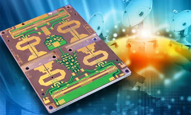
Antenna PCBs play a crucial role in wireless communication, enabling the reception and transmission of signals. With the advent of 5G networks, the demand for Antenna PCBs has significantly increased. They are extensively utilized in the telecommunications industry, supporting the rapid expansion of the Internet of Things (IoT) and facilitating seamless connectivity among electronic devices.
Please reach out to [email protected] for further information on pricing and manufacturing details for Antenna PCBs.
Antenna Basics
An FPC antenna is characterized by an exposed conductor that can act as an antenna when certain conditions are met, such as matching the signal’s wavelength or its multiples. This phenomenon is known as resonance, where the electrical energy fed to the antenna gets radiated into space.
The design of an antenna on a PCB involves two crucial aspects: the antenna feed and the antenna length. In PCBs, the antenna, typically a quarter-length conductor, can achieve performance similar to a dipole antenna. This is accomplished by placing a ground plane at a certain distance below the conductor to create an image of the same length (a quarter wavelength). Together, these sections function as dipole antennas and are known as quarter-wave monopoles.
When developing a PCB antenna design or a quarter-wave antenna, several considerations should be taken into account. These include the antenna feed mechanism, the length of the antenna, different types of antennas, as well as the size and shape of the return path and ground plane.
Antenna Categories
Antennas can be broadly categorized into three main types: wire antennas, PCB antennas, and chip antennas.
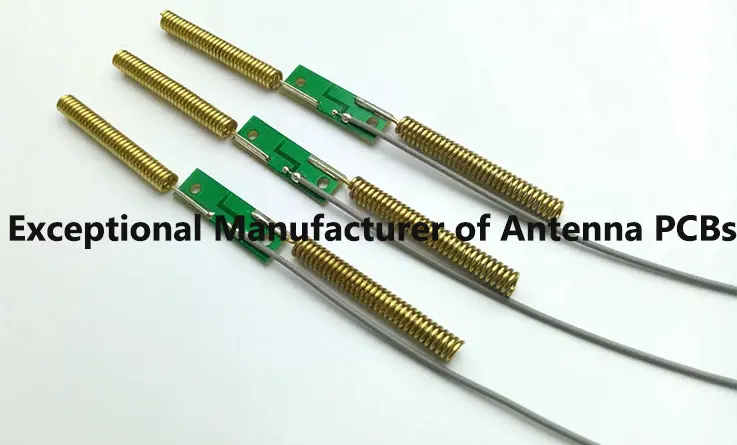
Wire Antennas: These antennas consist of a wire that extends from the printed circuit board into free space. They are designed to have a length that matches a quarter-wavelength over a ground plane and are typically fed using a 50-Ω four transmission line. Wire antennas provide excellent RF range and performance due to their three-dimensional exposure and specific dimensions. Wire antennas can take the form of loops, straight wires, or helix shapes.
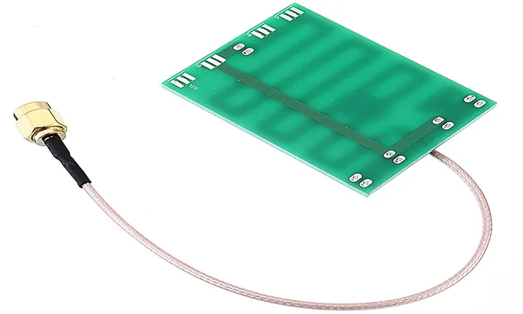
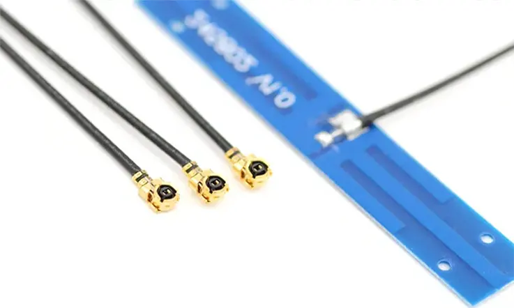
PCB Antennas: Also known as PCB trace antennas, these antennas are created by drawing traces on the printed circuit board. PCB antennas can have various shapes, including meandered traces, straight traces, circular traces, inverted F-type traces, or wiggly curves, depending on the available space and antenna constraints. Unlike wire antennas, PCB antennas are two-dimensional structures within the PCB plane. However, certain guidelines must be followed when converting a 3D antenna into a 2D PCB trace.
PCB antennas provide several advantages such as compact size, lower cost, and ease of manufacturability. However, they generally require more board space and have lower efficiency compared to wire antennas. Despite these limitations, PCB antennas can still offer an acceptable wireless range for Bluetooth Low Energy (BLE) applications.
Chip Antennas: Chip antennas are miniature integrated circuits with a conductor, designed specifically to be used when there is limited space for PCB antenna printing or to support 3D wire antennas. These tiny form-factor antennas are commonly employed in situations where size is a critical factor.
Before starting the design process for an antenna, especially for Bluetooth applications, it is crucial to consider the three main categories of antennas, their fundamental principles, and the different types available within each antenna class.
Understanding the Antenna PCB
Wireless technology has become increasingly prevalent in today’s world, with a wide range of electronic devices, such as smartphones, laptops, and tablets, relying heavily on wireless capabilities. An essential component that enables the transmission and reception of electromagnetic radiation in unrestricted space is the antenna PCB.
The PCB antenna, often found on printed circuit boards, is created by printing copper ink onto the board and establishing an electrical connection with other electronic components like connectors or resistors. This allows the antenna to transmit and receive electromagnetic waves. The antenna PCB plays a crucial role as a wireless device, responsible for the transmission and reception of signals. It finds diverse applications, primarily within the telecommunication sector.
The increasing prominence of 5G technology in the telecommunication sector further emphasizes the importance of antenna circuit boards, as more electronic devices will require these printed circuit boards to facilitate communication, particularly in the context of the Internet of Things (IoT).
Given this context, it becomes essential for electronics designers to have a comprehensive understanding of various aspects of antenna PCBs, specifically focusing on LPWAN (Low Power Wide Area Network) or LoRa PCB antennas. Such knowledge is necessary to effectively design and implement wireless communication systems.
What Is antenna PCB?
An antenna PCB refers to a printed circuit board (PCB) that integrates an antenna within its design. It combines the functionality of a PCB, which provides electrical connections and circuitry, with the capabilities of an antenna, which facilitates wireless communication by transmitting and receiving signals.
The antenna PCB is designed to efficiently radiate or capture electromagnetic waves, allowing devices to establish wireless connections for various applications, such as mobile communication, IoT devices, wireless sensors, and more. By incorporating the antenna directly into the PCB, it offers a compact and integrated solution for wireless communication needs.
Types of Antenna PCB
PCB antennas are integral components of high-frequency PCBs, serving as essential elements for wireless communication. They come in diverse types and are attached to the PCB. Here is a breakdown of the various types of PCB antennas:
Internal PCB Antennas:
Microstrip Antennas: These antenna designs use a metallic trace pattern on the PCB’s surface layer to generate and radiate RF signals.
Patch Antennas: Consisting of a radiating patch structure on the surface of the PCB, they provide low-profile, compact solutions.
Slot Antennas: Utilize slots or gaps in the PCB’s conductive layers to generate electromagnetic waves.
Planar Inverted-F Antennas (PIFAs): Incorporate a compact, meandered or folded element that extends above the PCB surface.
External PCB Antennas:
Monopole Antennas: Consist of a single conducting element extending outwards from the PCB surface, often used in wireless devices.
Dipole Antennas: Comprised of two conducting elements, they are commonly used in radio and Wi-Fi applications.
Yagi-Uda Antennas: Consist of a driven element and multiple parasitic elements arranged in a specific pattern for enhanced directivity.
Planar Antennas:
Planar Inverted-L Antennas (PILAs): Combine a planar conductive strip and a vertical component, forming an L-shaped structure.
Planar Helix Antennas: Utilize a planar spiral structure to create a helical antenna, offering circular polarization.
Slot Planar Antennas: Employ slots cut into the PCB to create radiation patterns and desired impedance characteristics.
Planar Log-Periodic Antennas (PLPAs): Designed with a planar array of radiating elements, covering a wide frequency range.
Integrated Antenna PCBs:
Printed Monopole Array: Consist of multiple monopole antennas arranged in an array to achieve enhanced performance.
Printed Dipole Array: Similar to the printed monopole array, but with multiple dipole antennas arranged in an array configuration.
Specialized Antenna PCBs:
RFID Antennas: Designed specifically for radio frequency identification (RFID) applications, enabling wireless identification and data transfer.
GNSS Antennas: Used for Global Navigation Satellite Systems (GNSS) such as GPS, GLONASS, Galileo, or BeiDou, to receive positioning signals.
It’s important to note that these categories are not exhaustive, and there can be variations and combinations of antenna types depending on specific design requirements and technological advancements.
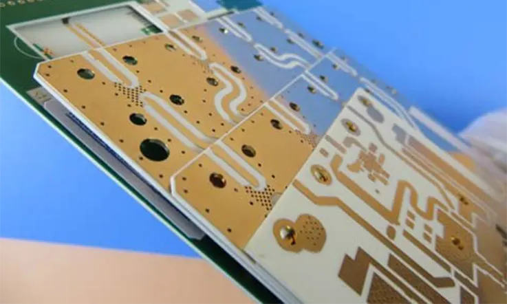
Factors to Consider When Choosing Antenna PCB Materials
The choice of materials for antenna PCBs depends on several factors, including the desired performance, frequency range, manufacturing process, and cost considerations. Here are some commonly used materials for antenna PCBs:
FR-4: This is the most widely used material for PCBs, including antenna PCBs. It is a flame-resistant epoxy-based laminate that offers good electrical insulation and mechanical strength. FR-4 is cost-effective and suitable for lower-frequency applications.
Rogers: Rogers Corporation is a leading manufacturer of high-frequency laminates specifically designed for RF and microwave applications. These materials provide excellent electrical performance, low dielectric loss, and stable performance at high frequencies. Rogers materials like RT/duroid and RO4000 series are commonly used for antenna PCBs.
Ceramic:Ceramic-based PCB materials, such as alumina (Al2O3) or aluminum nitride (AlN), are known for their excellent thermal conductivity and high-temperature stability. They are often used in high-power and high-frequency applications where heat dissipation and performance stability are critical.
PTFE (Polytetrafluoroethylene): PTFE-based materials, such as Teflon, offer low dielectric constant, low loss tangent, and excellent stability across a wide frequency range. They are commonly used in high-frequency applications, including antennas, due to their low signal loss and consistent performance.
Flexible Materials: For applications where flexibility is required, flexible PCB materials like polyimide (PI) are used. These materials allow the antenna PCB to conform to curved or non-planar surfaces, enabling integration in space-constrained and complex designs.
It’s important to note that the material selection depends on the specific requirements of the antenna design, including frequency range, impedance matching, signal quality, form factor, and cost constraints. Therefore, choosing the right material is crucial to ensure optimal antenna performance and overall system efficiency.
How to Design A Antenna Printed Circuit Boards ?
Designing an antenna printed circuit board (PCB) involves several steps. Here is a simplified outline of the process:
Define antenna requirements: Determine the specifications of your antenna such as frequency, gain, bandwidth, polarization, and form factor.
Choose antenna type: Select the appropriate type of antenna, such as patch antenna, dipole antenna, or helical antenna, based on your requirements and the application.
Determine PCB layout: Decide the size and shape of the PCB layout based on the antenna type and desired performance. Consider factors like ground plane size, clearance from other components, and manufacturing constraints.
Design antenna elements: Use antenna design software or simulation tools to design the antenna elements, such as radiating elements, feed lines, and matching networks. Optimize the design for desired performance metrics.
Incorporate ground plane: Ensure a well-designed ground plane that provides a stable reference for the antenna and minimizes interference.
Optimize impedance matching: Use impedance matching techniques to maximize power transfer between the antenna and RF circuitry. This may involve adding components like baluns, matching networks, or transmission lines.
Test and prototype: Build a prototype of the PCB antenna and conduct tests for performance evaluation. Measure parameters like return loss, radiation patterns, and gain.
Iterative refinement: Based on test results, make adjustments to the design to improve performance. This may involve modifying the antenna geometry, adjusting matching components, or optimizing the ground plane.
Manufacture the PCB: Once the design is finalized, generate the Gerber files or other manufacturing files required for PCB fabrication. Choose a reliable PCB manufacturer to produce the antenna PCB.
Assemble and integrate: Receive the fabricated PCB and assemble it with the required components in the final product or system. Ensure proper mounting and connection of the antenna.
Note that designing antennas can be a complex process and often requires expertise in RF engineering. It may be beneficial to involve an experienced RF engineer or consult specialized resources or literature for more detailed guidance during the design process.
Factors to Consider to Manufacture Antenna PCB
When manufacturing an antenna PCB, several factors need to be considered to ensure the successful production of a high-quality and functional product. Here are some important factors to consider:
Material selection: Choose the appropriate substrate material for your antenna PCB based on factors such as frequency range, dielectric constant, loss tangent, thermal properties, and manufacturing feasibility. Common materials include FR-4, Rogers, or specialty materials designed for high-frequency applications.
PCB stack-up: Determine the layer count and stack-up configuration based on the specific requirements of your antenna design. Consider factors such as signal integrity, impedance control, and isolation between layers to optimize performance.
Copper thickness: Select an appropriate copper thickness for the antenna traces and ground plane based on the desired electrical performance and manufacturing capabilities. Thicker copper layers can provide better signal integrity and heat dissipation.
Antenna placement and clearance: Ensure proper layout and clearance around the antenna components to minimize interference and maintain desired radiation patterns. Consider the proximity of other components, especially those that emit electromagnetic interference (EMI).
Ground plane design: Design an effective ground plane for the antenna to serve as a reference and provide shielding against EMI. Consider factors such as size, shape, and placement to maximize performance and minimize impedance mismatches.
Manufacturing capabilities: Evaluate the manufacturing capabilities of the PCB manufacturer to ensure they can meet your design requirements. Consider factors such as minimum trace width and spacing, minimum drill size, aspect ratio limitations, and other specifications relevant to your antenna design.
Impedance control: Specify tight impedance tolerances for critical transmission lines and impedance-matched areas of the PCB to ensure proper signal integrity and power transfer. This is particularly important for RF and microwave applications.
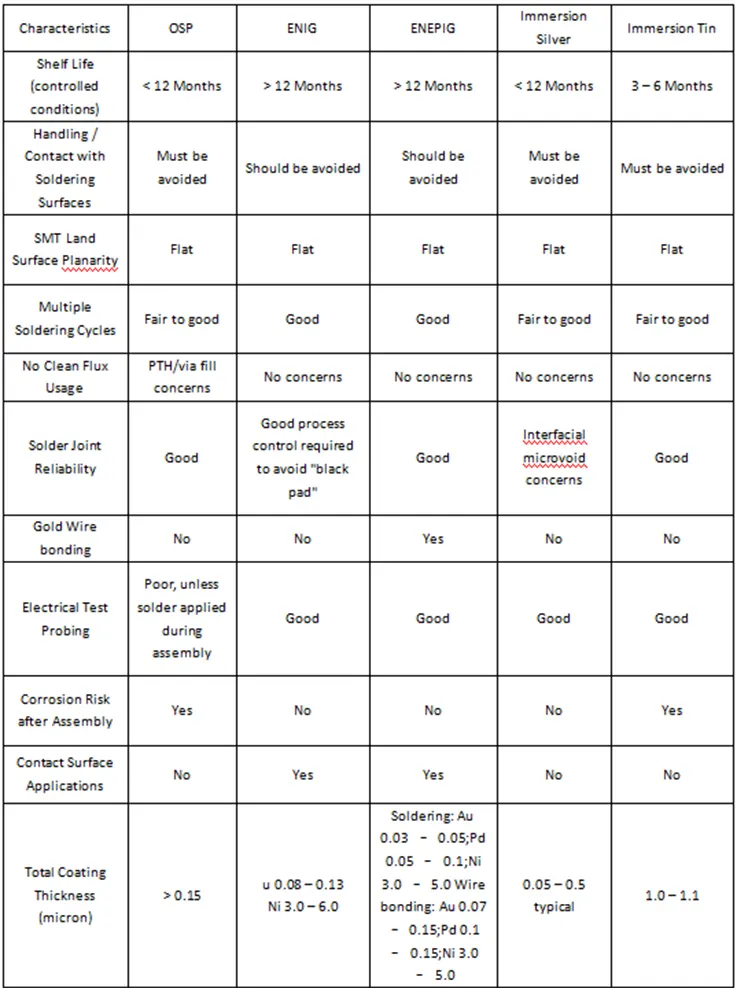
Surface finish: Choose an appropriate surface finish for the PCB based on your application requirements. Common options include HASL, ENIG, immersion tin, OSP, or silver. Consider factors such as solderability, corrosion resistance, and compatibility with lead-free soldering processes.
Design for manufacturability (DFM): Design the antenna PCB with manufacturability in mind by adhering to industry-standard design rules, avoiding complex or problematic features, and ensuring proper documentation and notes for clarity.
Testing and inspection: Plan for thorough testing and inspection of the manufactured antenna PCBs to verify their functionality and performance. Consider performing tests like continuity testing, RF testing, impedance measurement verification, and visual inspection to ensure quality.
By considering these factors, you can optimize the manufacturing process and increase the likelihood of a successful and reliable antenna PCB. Collaboration with an experienced PCB manufacturer or RF engineer can also provide valuable insights and guidance throughout the manufacturing process.
Challenges and Solutions of Antenna PCBs
In the context of antenna PCB design, some common challenges and potential solutions include:
Miniaturization and Size Constraints:
Challenge: Limited available space for the antenna on the PCB.
Solution: Exploring compact antenna designs such as planar, meandered, or chip antennas. Additionally, employing techniques like fractal or metamaterial structures can help achieve miniaturization.
Bandwidth and Frequency Range:
Challenge: Achieving sufficient bandwidth and covering the desired frequency range.
Solution: Optimizing the antenna geometry, such as using multiple resonant elements, adding matching networks, or incorporating tunable components to enhance the operating bandwidth and frequency range.
Radiation Efficiency:
Challenge: Ensuring a high level of radiation efficiency to maximize the power transmission or reception.
Solution: Careful design considerations, including selecting appropriate materials for the PCB, minimizing losses due to conductor resistivity, utilizing well-matched impedance, and reducing the influence of surrounding components or structures.
Environmental Effects:
Challenge: Antenna performance degradation caused by environmental factors like nearby objects, electromagnetic interference, or varying conditions.
Solution: Conducting extensive EMC/EMI testing to identify potential environmental challenges, employing shielding techniques, adding filters, implementing polarization diversity, or utilizing adaptive algorithms to mitigate the effects of changing conditions.
Manufacturing Considerations:
Challenge: Ensuring manufacturability and consistent performance during production.
Solution: Collaborating with PCB manufacturers to optimize the antenna design for manufacturing processes, considering material properties, fabrication tolerances, and validation testing to ensure consistent performance across production units.
These challenges and solutions provide a glimpse into the considerations involved in antenna PCB design. However, it’s important to note that the specific challenges and solutions can vary depending on the application, frequency range, desired performance, and other project-specific factors.
Future Trends and Developments
Future trends and developments in antenna PCB design are likely to focus on the following areas:
5G and Beyond:
As 5G networks continue to expand and evolve, there will be a need for antenna PCB designs that support higher frequencies, wider bandwidths, and more advanced beamforming and MIMO techniques to enhance data rates and network coverage.
Integrated Multiband Antennas:
With the increasing demand for connected devices operating in multiple frequency bands, there will be a push towards integrated multiband antennas on PCBs. These antennas will allow for simultaneous operation across different wireless standards, such as cellular, Wi-Fi, Bluetooth, and GPS.
Millimeter-wave Antennas:
Millimeter-wave frequencies (above 30 GHz) are being explored for applications like high-speed wireless communication, automotive radar, and imaging systems. Future developments will focus on optimizing antenna designs for these higher frequencies and addressing the challenges associated with propagation characteristics and antenna integration.
Flexible and Wearable Antennas:
Antennas that can conform to irregular surfaces or be integrated into flexible and wearable devices will be a key area of development. This includes using flexible PCB materials, conductive textiles, or printed antenna technologies to enable seamless integration while maintaining performance.
Antenna-in-Package (AiP) Integration:
AiP integration involves embedding antennas within integrated circuit (IC) packages or modules. This approach enhances miniaturization, reduces losses, and improves overall system performance. Future developments will focus on optimizing AiP designs for different applications and integrating multiple functions within a single package.
Advanced Simulation and Design Tools:
The development of more advanced simulation and design tools will enable more accurate modeling and optimization of antenna PCB designs. These tools will consider factors like material properties, non-linear effects, 3D electromagnetic simulations, and optimization algorithms to enhance performance and streamline the design process.
Smart Antenna Systems:
Future antenna PCB designs may incorporate smart antenna systems with advanced signal processing techniques. This includes adaptive beamforming, spatial filtering, and cognitive radio capabilities to dynamically optimize antenna performance in complex wireless environments.
These trends indicate the potential directions for future developments in antenna PCB design, driven by the increasing demand for high-speed wireless communication, IoT devices, smart cities, and emerging technologies like autonomous vehicles and augmented reality.
Conclusion
Antenna PCB design plays a crucial role in enabling wireless communication and connectivity in various devices and systems. The challenges and solutions involved in antenna PCB design include miniaturization and size constraints, achieving sufficient bandwidth and frequency range, ensuring high radiation efficiency, addressing environmental effects, and considering manufacturing considerations.
Antenna PCB design is expected to be driven by trends such as the expansion of 5G and beyond, the integration of multiband antennas, the exploration of millimeter-wave frequencies, the development of flexible and wearable antennas, the integration of antennas within IC packages, the advancement of simulation and design tools, and the adoption of smart antenna systems.
These future trends and developments will contribute to improved wireless connectivity, enhanced performance, and increased functionality in a wide range of devices and applications. As technology continues to evolve, antenna PCB design will continue to play an essential role in enabling seamless communication and connectivity in our increasingly connected world.
Regardless of your intended use for a Bluetooth device, the ability to quickly establish a pairing connection is essential. For instance, if you wish to enjoy your favorite music during your vacation, it’s wise to bring along a Bluetooth speaker capable of playing your playlists for extended periods. Similarly, if you want to transfer some impressive selfies to your friend’s cellphone, you can accomplish this by activating the Bluetooth connection and sending the images via the link.
Bluetooth technology has become ubiquitous, enabling various functionalities facilitated by Bluetooth circuit boards. This article offers an in-depth exploration of Bluetooth circuit boards, including their types and applications.
The initial chapter provides a brief overview of Bluetooth technology before delving into the intricate details of Bluetooth circuit boards themselves.
Bluetooth Technology
Bluetooth technology is a wireless communication protocol that enables short-range data transmission between devices. It uses radio waves within the 2.4 GHz frequency band to establish connections between devices like smartphones, computers, speakers, headphones, and IoT devices.
Key features of Bluetooth Technology Include
Pairing: Bluetooth devices establish a secure connection by pairing with each other. Pairing involves exchanging authentication and encryption keys to ensure a secure and private connection.
Profiles: Bluetooth profiles define specific functionalities and capabilities for different types of devices. Common profiles include Hands-Free Profile (HFP), Advanced Audio Distribution Profile (A2DP), and Human Interface Device (HID) profile.
Range: Bluetooth has a typical range of up to 10 meters, known as Class 2 devices. Bluetooth Class 1 devices can have an extended range of up to 100 meters.
Data Transfer: Bluetooth supports various data transfer modes, including asynchronous data transfer (ACL) for sending larger amounts of data and synchronous connection-oriented (SCO) for real-time audio.
Low Energy: Bluetooth Low Energy (BLE) is a power-efficient version of Bluetooth that enables devices to operate on battery power for extended periods. It is widely used in wearable devices, healthcare applications, and IoT devices.
Compatibility: Bluetooth technology is backward compatible, allowing newer Bluetooth devices to connect and communicate with older ones. However, the features and capabilities may vary depending on the supported Bluetooth version.
Security: Bluetooth technology incorporates security measures like encryption and authentication to protect data transmission and prevent unauthorized access.
Bluetooth technology has become ubiquitous, providing convenient wireless connectivity for a wide range of devices, including smartphones, audio peripherals, smart home devices, wearable technology, and more. It continues to evolve with each new version, offering improved performance, higher data rates, and enhanced features for seamless device connectivity.
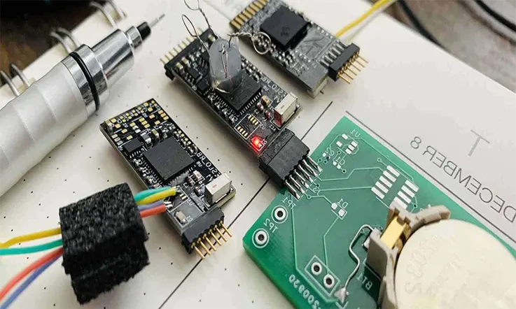
What is Bluetooth Circuit Board?
A Bluetooth circuit board, also known as a Bluetooth module or Bluetooth chip, is an electronic component that integrates the Bluetooth technology into a compact circuit board. It is designed to facilitate wireless communication between devices using Bluetooth technology.
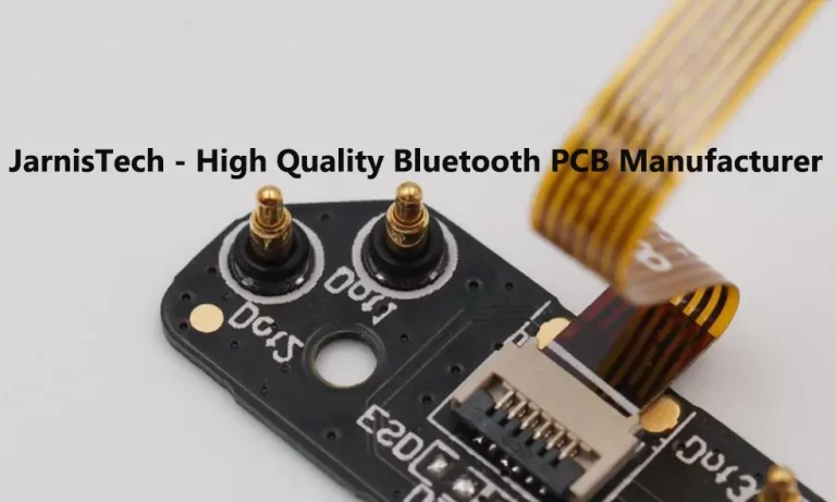
The Bluetooth circuit board typically consists of several key components, including a Bluetooth transceiver, antenna, microcontroller, and necessary support circuitry. The transceiver is responsible for transmitting and receiving Bluetooth signals, while the antenna facilitates wireless connectivity. The microcontroller handles the data processing and manages the communication protocols.
Bluetooth circuit boards come in various form factors, such as surface mount modules, system-on-chip (SoC) modules, or stand-alone modules. They can be embedded in various devices, such as smartphones, tablets, laptops, wireless headphones, speakers, smartwatches, and other IoT (Internet of Things) devices.
The Bluetooth circuit board enables these devices to establish short-range wireless connections with other compatible Bluetooth-enabled devices. It allows for data transmission, audio streaming, device pairing, and control functionalities, making it a versatile technology for wireless communication in numerous applications.
Types of Applications of Bluetooth Circuit Board
Bluetooth circuit boards find application in various domains and industries. Some common applications of Bluetooth circuit boards include:
Consumer Electronics: Bluetooth-enabled devices, such as smartphones, laptops, headphones, speakers, and smartwatches, rely on Bluetooth circuit boards to enable wireless connectivity, data transfer, and audio streaming between devices.
Home Automation: Bluetooth circuit boards are used in home automation systems to connect and control smart devices, such as lights, thermostats, door locks, and security systems. They allow for convenient wireless control and monitoring within a home network.
Automotive: Bluetooth circuit boards are integrated into car infotainment systems, enabling hands-free calling, audio streaming, and wireless connectivity with smartphones. They also facilitate features like Bluetooth-enabled keyless entry and vehicle diagnostics.
Healthcare: Bluetooth circuit boards are utilized in healthcare devices for data monitoring and tracking. For example, wearable fitness trackers, blood glucose monitors, and heart rate monitors incorporate Bluetooth technology to transmit health-related data to smartphones or other compatible devices.
Industrial Automation: Bluetooth circuit boards play a role in industrial applications, such as wireless sensors, equipment monitoring, and control systems. They provide wireless connectivity and data exchange between devices in industrial automation environments.
IoT (Internet of Things): Bluetooth circuit boards are important components in IoT devices that rely on wireless communication. They enable connectivity and data exchange between interconnected IoT devices, creating a cohesive IoT ecosystem.
Gaming: Bluetooth circuit boards are used in gaming consoles, controllers, and accessories to establish wireless connections and enable multiplayer gaming experiences across different devices.
These are just a few examples, and Bluetooth circuit boards have a wide range of applications beyond these industries. Their versatility and compatibility make them a widely adopted technology for wireless communication and connectivity.
Key Considerations of Designing a Bluetooth PCB
Designing a Bluetooth PCB (Printed Circuit Board) involves the following key considerations:
Bluetooth Module Selection: Choose a suitable Bluetooth module that meets the requirements of your application. Consider factors such as range, power consumption, data rate, supported Bluetooth profiles, and integration options.
RF Layout Design: Pay close attention to the RF circuit layout, considering factors like trace length, impedance matching, and signal integrity. Place the Bluetooth module and associated components carefully to minimize signal loss and interference.
Antenna Design and Placement: Determine the type of antenna that suits your application, such as chip antennas, trace antennas, or external antennas. Ensure proper clearance around the antenna, avoid nearby metallic objects, and optimize the antenna placement for optimal signal strength and range.
Power Supply and Decoupling: Provide stable and clean power to the Bluetooth module, ensuring appropriate voltage levels and noise reduction. Use suitable decoupling capacitors near the power supply pins of the module to filter out noise and maintain a stable power source.
Signal Integrity: Implement good PCB design practices to maintain signal integrity. Minimize noise coupling, use proper ground planes and power planes, and apply impedance matching techniques where necessary.
EMI/EMC Considerations: Pay attention to electromagnetic interference (EMI) and electromagnetic compatibility (EMC) requirements. Implement EMI shielding techniques, use proper grounding, and follow PCB layout guidelines to mitigate EMI/EMC issues.
Mechanical Constraints: Consider mechanical constraints, such as the size, shape, and mounting requirements of your Bluetooth PCB. Ensure that the PCB fits within the desired enclosure and aligns with mechanical components such as connectors, buttons, and indicators.
Testing and Prototyping: Plan for testing and prototyping stages to validate the Bluetooth PCB design. Verify functionality, RF performance, power consumption, and compliance with relevant standards and regulations.
Documentation and Manufacturing Files: Prepare comprehensive documentation, including schematics, layout files, bill of materials (BOM), and assembly drawings, to facilitate the manufacturing process.
It is crucial to follow Bluetooth design guidelines provided by the module manufacturer and consult relevant design resources and standards, such as the Bluetooth SIG (Special Interest Group) specifications, to ensure a reliable and robust Bluetooth PCB design. Additionally, collaborating with experienced RF engineers or PCB designers can provide valuable insights and expertise for successful Bluetooth PCB design.
Manufacturing Bluetooth PCBs Step
Manufacturing Bluetooth PCBs (Printed Circuit Boards) typically involves the following steps:
PCB Fabrication
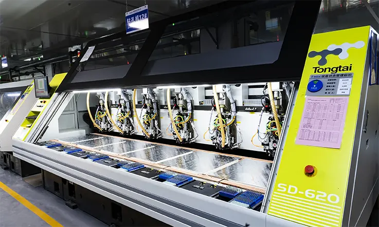
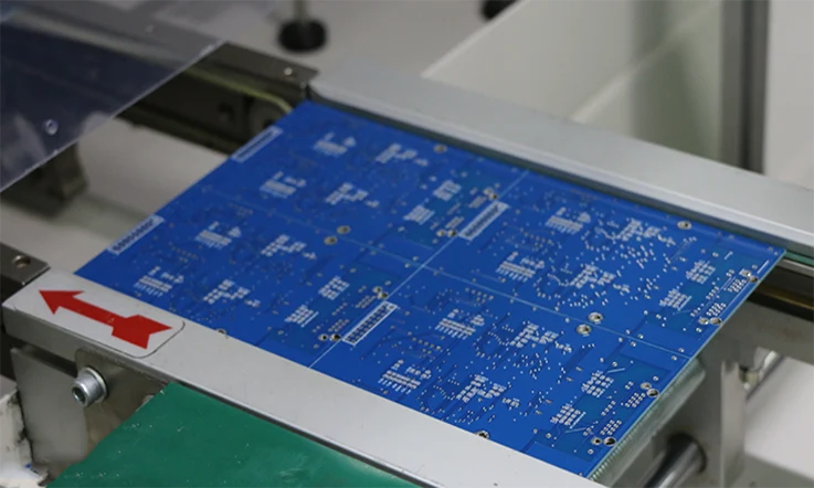
Start by generating the manufacturing files, including Gerber files that contain the PCB layout information. Provide these files to a PCB manufacturer or fabrication house. The manufacturer will use the files to produce the PCBs according to your design specifications. The fabrication process involves processes like layer alignment, copper deposition, etching, drilling, and solder mask application.
Component Sourcing
Source the required electronic components for your Bluetooth PCB. This includes the Bluetooth module, passive components (resistors, capacitors, etc.), connectors, and any other specific components needed for your design. Choose reputable component suppliers or distributors to ensure component authenticity and quality.
PCB Assembly
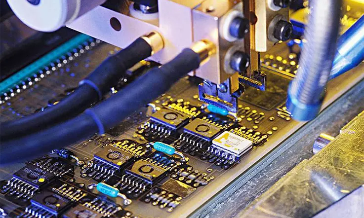
The process of assembling components onto the PCB is known as PCB assembly or manufacturing. This can be done in-house if you have the necessary equipment and expertise, or you can outsource it to a contract manufacturer (CM) or electronic manufacturing services (EMS) provider. The assembly process typically involves the following steps:
a. Solder Paste Stencil: A stencil is used to apply solder paste onto the PCB, defining the locations where components will be placed.
b. Pick and Place: Automated pick-and-place machines accurately place surface-mount components onto the solder paste on the PCB. This includes the Bluetooth module, resistors, capacitors, ICs, and other components.
c. Soldering: After component placement, the PCB goes through a reflow soldering process where heat is applied to melt the solder paste, creating a permanent electrical connection between the components and the PCB.
d. Inspection and Testing: Visual inspection, automated optical inspection (AOI), and/or X-ray inspection are performed to ensure the quality of the solder connections. Functional testing may also be conducted to verify the functionality of the Bluetooth circuitry.
Quality Assurance and Testing
Quality control measures are taken to ensure the manufactured Bluetooth PCBs meet the required standards and specifications. This may include electrical testing, functional testing, and performance testing of the Bluetooth functionality.
Packaging and Shipping
Once the manufacturing and testing processes are complete, the Bluetooth PCBs are packaged securely to protect them during transportation. They are then shipped to the desired destination.
It’s important to work closely with the PCB manufacturer and assembly provider to ensure clear communication, provide detailed documentation, and address any specific requirements or considerations for the Bluetooth PCB manufacturing process.
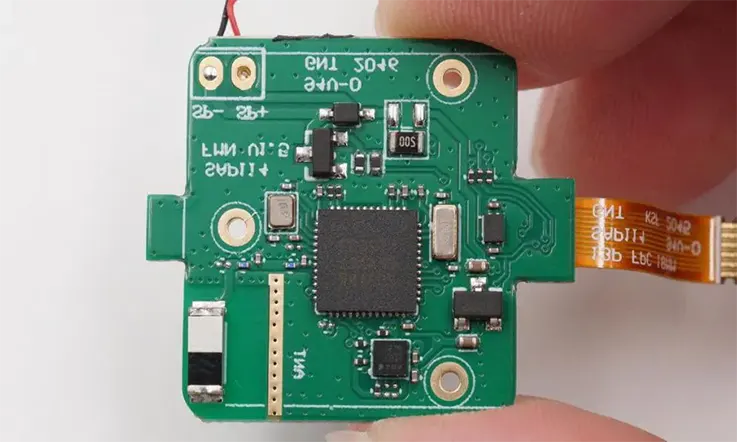
Components of a Bluetooth Circuit Board
A Bluetooth circuit board consists of various components that work together to enable wireless communication using Bluetooth technology. The key components typically found on a Bluetooth circuit board include:
Bluetooth Transceiver: The Bluetooth transceiver is responsible for transmitting and receiving Bluetooth signals. It converts data into radio waves for transmission and demodulates received radio waves into usable data.
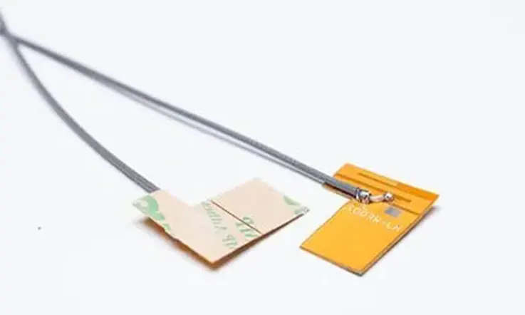
Antenna: The antenna is essential for wireless connectivity. It is used to send and receive Bluetooth signals between devices. The type and design of the antenna can vary depending on the specific application and range requirements.
Microcontroller (MCU): The microcontroller acts as the brain of the Bluetooth circuit board. It handles the data processing, manages communication protocols, and controls the overall operation of the Bluetooth module. The MCU also interfaces with other components on the circuit board.
Support Circuitry: The Bluetooth circuit board includes additional circuitry to support its operation. This may include voltage regulators, filters, oscillators, and capacitors. These components ensure stable power supply, frequency stability, and noise reduction for optimal performance.
Memory: Bluetooth circuit boards often have integrated memory to store firmware, configuration data, and other necessary information for operation. The memory can be in the form of flash memory or EEPROM (Electrically Erasable Programmable Read-Only Memory).
Interfaces: Bluetooth circuit boards typically have interfaces for connecting to external devices or systems. This can include UART (Universal Asynchronous Receiver-Transmitter) for serial communication, SPI (Serial Peripheral Interface) or I2C (Inter-Integrated Circuit) for interfacing with other devices, and GPIO (General-Purpose Input/Output) pins for general-purpose connections.
Power Supply: Bluetooth circuit boards require a power supply to operate. They may include voltage regulation circuitry to ensure stable power to the components. The power supply can come from batteries, USB ports, or other power sources depending on the specific application.
These components work together to enable wireless communication and functionality provided by Bluetooth technology. The specific configuration and components can vary depending on the design and purpose of the Bluetooth circuit board.
How To Find High quality Bluetooth Circuit Boards Manufacturer?
To find a high-quality Bluetooth circuit board manufacturer, you can follow these steps:
Research and compile a list: Start by conducting online research to identify potential manufacturers. Look for companies with a strong reputation, positive customer reviews, and a track record of producing high-quality products.
Assess their experience and expertise: Check the manufacturer’s website or contact them directly to gather information about their experience in producing Bluetooth circuit boards. Look for their specialization in electronic manufacturing and inquire about their expertise in Bluetooth technology.
Quality certifications: Determine if the manufacturer holds relevant quality certifications such as ISO 9001 or IPC standards. These certifications indicate their commitment to maintaining high-quality standards in their manufacturing processes.
Request samples: Ask the manufacturer if they can provide samples of Bluetooth circuit boards they have previously produced. Evaluate the quality and reliability of these samples to assess whether they meet your requirements.
Inquire about production capabilities: Discuss the manufacturer’s production capabilities in terms of volume, lead times, and capacity to ensure they can meet your specific requirements.
Cost and pricing structure: Obtain quotes from multiple manufacturers and compare their pricing structures. Be cautious of unusually low prices, as they may indicate compromises in quality or reliability.
Communication and responsiveness: Evaluate the manufacturer’s level of communication and responsiveness. A reliable manufacturer should be proactive in addressing your inquiries and providing updates throughout the production process.
Additional services: Consider whether the manufacturer offers additional services such as design assistance, prototyping, customization options, and technical support. These services can be valuable for ensuring the success of your Bluetooth circuit board project.
References and reviews: Request references from the manufacturer and reach out to their previous clients for feedback on their experience working with the manufacturer. Online reviews and testimonials can also provide valuable insights.
Visit the facility (optional): If feasible, consider visiting the manufacturer’s facility to observe their operations firsthand and assess their manufacturing processes and quality control measures.
By following these steps, you can identify a high-quality Bluetooth circuit board manufacturer that meets your specific requirements and standards.
Your Professional Bluetooth PCB Manufacturer – JarnisTech
Why More Than 3000 Clients Over the WorldLove to Work with Us:
Customized Design
JarnisTech specializes in the production of multi-layer circuit boards, offering a comprehensive range of services to cater to diverse client requirements. Our extensive service scope encompasses PCB design, circuit simulation, and PCB design technology training. We also provide assistance in schematic component library design, PCB packaging library design, as well as consultation on PCB processing and inspection techniques. Furthermore, we are well-versed in SMT (Surface Mount Technology) and reflow soldering technology, providing expert guidance and support in these areas. By leveraging our expertise and resources, we aim to deliver superior solutions tailored to the specific needs of our valued clients.
Quality Control
At JarnisTech, we hold an unwavering commitment to delivering products of the highest quality to our esteemed customers. To ensure this, we have meticulously implemented the ISO9001 quality system and diligently adhere to stringent quality protocols. Our overarching objective is to eliminate the production of defective products altogether. Hence, we rigorously enforce a zero-tolerance policy that entails not producing, accepting, or manufacturing any items that fall short of our rigorous quality standards. We firmly believe that quality is a result of the dedicated efforts of our skilled workforce and not merely reliant on testing procedures. By prioritizing excellence at every stage of our operations, we strive to exceed customer expectations and maintain our reputation as a provider of top-tier quality products.
Fast Delivery Time
JarnisTech is a trusted provider of comprehensive printed circuit board and assembly solutions, catering to a wide range of client needs. Our extensive product line encompasses express prototype services as well as quick turn mass production capabilities. Notably, we understand the importance of urgent prototype board orders and prioritize swift execution. In this regard, we offer expedited production within 24 to 48 hours, ensuring prompt delivery facilitated by reputable shipping carriers such as UPS, DHL, and FedEx. Rest assured, our streamlined processes and efficient service will seamlessly integrate with your production schedule, minimizing any disruptions.
One- Stop Solution for You
JarnisTech provides a comprehensive suite of services encompassing PCB layout and design, electronic components sourcing, PCB manufacturing, and assembly. By offering a one-stop solution, we eliminate the need for engaging multiple suppliers for various project requirements. Moreover, our experienced engineers are equipped to offer valuable insights and guidance throughout the design phase of your product, ensuring efficient resource allocation and time-saving advantages. As a result, we strive to optimize cost-effectiveness while delivering exceptional quality and convenience to our clients.
One Professional and Exprienced Team
At JarnisTech, our team comprises seasoned professionals who are recognized as industry experts in their respective fields. With a wealth of experience exceeding 20 years, our engineering and technical personnel have honed their skills while working in prominent manufacturing facilities involved in PCB fabrication, assembly, and components sourcing. This extensive expertise enables us to deliver prompt and proficient PCB solutions, ensuring the utmost satisfaction of our valued customers.
Advanced Equipments
At JarnisTech, we pride ourselves on utilizing cutting-edge equipment sourced from renowned manufacturers around the globe, including the United States, Germany, Japan, and other leading countries. Our commitment to delivering exceptional quality stems from our continual investment in acquiring state-of-the-art machinery. By staying at the forefront of technological advancements, we strive to meet and exceed the requirements of our valued clients.
Conclusion
When assembling Bluetooth circuit boards, it is crucial to uphold professional standards to ensure optimal functionality, range, and other key features. In this regard, we offer a reliable and experienced solution. With years of industry expertise, we specialize in collecting Bluetooth PCBs, guaranteeing high quality while adhering to your precise specifications.
By collaborating with us, you can benefit from the services of a trusted partner dedicated to providing exceptional Bluetooth circuit boards. Whether you require customized orders or bulk quantities, our team is well-equipped to meet your needs. Furthermore, we prioritize cost-effectiveness to support the growth of your business.
To avail yourself of our services and secure Bluetooth PCBs that meet your requirements, please don’t hesitate to get in touch with us. We look forward to the opportunity to serve you.
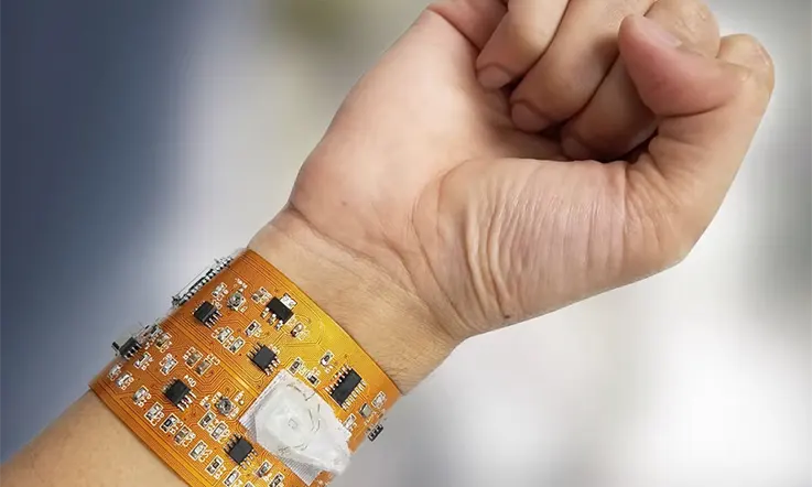
In recent years, the popularity of wearable devices has soared, propelled by remarkable advancements in the electronics industry and the availability of highly integrated electronic components that offer enhanced efficiency, performance, and compactness. At the core of each wearable device, whether it’s a smartwatch, fitness tracker, or electro-medical device (EMD), lies a printed circuit board (PCB) whose design presents a formidable challenge for electronic engineers. Creating a successful wearable device necessitates meeting a range of requirements, including small form factor, lightweight construction, low power consumption, reliability, and minimal heat generation.
Given their exceptionally compact size and relatively recent emergence in the market, there is no established standard specifically tailored to PCB design for wearable devices. However, it is possible to leverage techniques and recommendations that apply to circuits with similar characteristics, drawing on the expertise gained from the development and production of advanced PCBs.
Overview of Wearable Technology
Wearable technology refers to electronic devices that can be worn on the body, typically as accessories or clothing items. These devices are designed to provide functionality and connectivity while being convenient and seamlessly integrated into daily life.
Wearable technology has gained significant popularity in recent years due to advancements in miniaturization, sensor technology, wireless connectivity, and computing power. It has found applications in various fields, including fitness and health monitoring, communication, entertainment, fashion, and industrial sectors.
Key Features and Functions of Wearable Technology
Sensing and Monitoring: Wearable devices often incorporate sensors to monitor various aspects of the user’s body and environment. These sensors can include heart rate monitors, accelerometers, gyroscopes, GPS, temperature sensors, and more.
Data Collection and Analysis: Wearable devices collect data from the sensors and process it to provide meaningful insights to the user. This data can include activity levels, sleep patterns, biometric measurements, location information, and more.
Connectivity: Most wearable devices are equipped with wireless connectivity options such as Bluetooth, Wi-Fi, or cellular connectivity. This allows them to communicate with smartphones, tablets, or other devices, enabling data transfer, notifications, and remote control functionalities.
User Interface: Wearable devices utilize various user interface options to interact with the wearer. This can include touchscreens, buttons, voice commands, gestures, or a combination of these elements.
Integration with Mobile Devices and Applications: Many wearable devices are designed to work in tandem with smartphones or other mobile devices. They often have companion apps that enable data synchronization, customization, and extended functionalities.
Examples of Wearable Technology
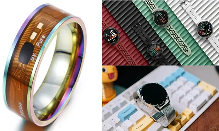
Fitness Trackers: These devices, such as fitness bands or smartwatches, monitor physical activities, track steps, calories burned, sleep patterns, and heart rate. They provide insights for fitness and health management.
Smartwatches: These wrist-worn devices offer features beyond timekeeping. They can display notifications, allow phone calls, track fitness metrics, control music playback, and run various apps.
Augmented Reality (AR) and Virtual Reality (VR) Headsets: These devices immerse users in virtual or augmented environments, providing an interactive and immersive experience for gaming, education, training, or entertainment purposes.
Smart Clothing: Certain garments incorporate sensors and electronic components for tracking biometrics, posture, or environmental factors. They can be used in sports, healthcare, or fashion industries.
Smart Glasses: These glasses feature built-in displays, cameras, and sensors, enabling hands-free access to information, navigation assistance, and augmented reality overlays.
Medical Wearables: Wearable devices in the medical field include devices for continuous glucose monitoring, blood pressure monitoring, sleep apnea tracking, and more.
The field of wearable technology is constantly evolving, with ongoing advancements in materials, battery life, connectivity, and functionality. It holds promising potential for enhancing personal well-being, improving productivity, and transforming various industries.
What Is wearable PCB?
A wearable PCB (Printed Circuit Board) refers to a circuit board that is specifically designed to be integrated into wearable devices, such as smartwatches, fitness trackers, smart clothing, and other wearable gadgets. PCBs are essential components of electronic devices as they provide a platform for connecting and mounting electronic components, such as microchips, sensors, and other circuitry.
In the context of wearables, PCBs are miniaturized and flexible to accommodate the unique form factors and requirements of wearable devices. They are typically lightweight, thin, and bendable to conform to the shape of the wearable product or fit within the available space. This flexibility allows PCBs to be integrated into garments, accessories, or directly onto the human body.
Wearable PCBs are designed to provide electrical connectivity between various components within the wearable device. They enable the transfer of power, data signals, and control signals between the microcontroller, sensors, display, battery, and other components. The PCB layout and design are optimized for efficient power consumption, reliable data transmission, and compactness.
Wearable PCBs often incorporate advanced technologies like surface mount components, ultra-thin conductive traces, and multi-layered designs to maximize functionality while minimizing size and weight. They may also integrate additional features like wireless connectivity (Bluetooth, Wi-Fi), charging circuits, and power management systems.
Overall, wearable PCBs play a crucial role in enabling the functionality and performance of wearable devices, allowing them to perform various tasks such as monitoring health data, tracking activity, displaying information, and connecting to other devices or networks.
Wearable PCB Types
Wearable PCBs (Printed Circuit Boards) can come in various types depending on the specific requirements and design considerations of the wearable device. Here are some common types of wearable PCBs:
Rigid PCBs
Rigid PCBs are the most common type of PCB used in wearables. They have a solid substrate made of rigid materials like fiberglass or epoxy resin. Rigid PCBs provide stability and support to the wearable device.
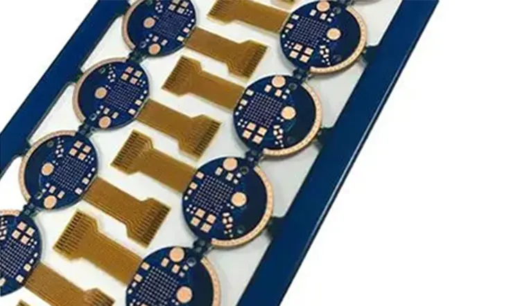
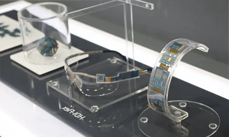
Flexible PCBs
Flexible PCBs are designed to bend and flex, making them suitable for wearable devices that require flexibility. They are made of flexible materials like polyimide or polyester. Flexible PCBs allow for shape conformity, making them ideal for wearables that need to conform to the body or an irregular surface.
Benefits of Flexible PCBs in Wearable Devices:
Size and Weight Reduction: Flexible PCBs can be designed to be thin, lightweight, and highly flexible, allowing them to conform to the shape of the wearable device. This property makes them ideal for space-constrained wearables where size and weight reduction are crucial factors.
Flexibility and Bendability: As the name suggests, flexible PCBs can be bent, twisted, and folded without damaging their functionality. This flexibility enables the design of wearable devices that can conform to the contours of the human body or fit into unconventional shapes.
Increased Reliability: Flexible PCBs have fewer interconnects and solder joints compared to rigid PCBs, reducing the risk of interconnection failures. The absence of connectors and cables also minimizes the likelihood of disconnections or breakages, enhancing the overall reliability of wearable devices.
Enhanced Durability: Wearable devices often encounter bending, stretching, or twisting motions during use. Flexible PCBs can withstand these mechanical stresses without compromising their electrical performance, leading to increased durability and longer product lifecycles.
Improved Thermal Management: Flexible PCBs have excellent thermal dissipation properties, allowing for efficient heat transfer. This feature is essential in wearables that generate heat, such as smartwatches or fitness trackers, ensuring proper functioning and preventing overheating.
Applications of Flexible PCBs in Wearable Devices:
Smartwatches: Flexible PCBs can be used in smartwatches to enable the display, touch sensors, microcontrollers, and other components to flex with the shape of the wristband. This ensures a comfortable fit and seamless integration of electronics into the device.
Fitness Trackers: Flexible PCBs are well-suited for fitness trackers due to their ability to conform to the contours of the body. They can be integrated into wristbands, chest straps, or other wearable forms, accommodating various sensors and connecting them to the main processing unit.
Medical Wearables: Flexible PCBs find applications in medical wearables like health monitoring devices, ECG monitors, and smart medical patches. Their flexibility allows for comfortable and non-intrusive integration into garments or adhesion to the skin, enabling continuous health monitoring.
Smart Clothing: Flexible PCBs can be integrated into smart clothing, such as sports apparel or safety garments. They enable the integration of sensors, LEDs, or communication modules while maintaining the flexibility and washability of the fabric.
Head-Mounted Displays (HMDs): Flexible PCBs play a crucial role in headsets or augmented reality glasses. They facilitate the connection of display panels, sensors, microcontrollers, and other components while maintaining the lightweight and ergonomic design required for comfortable use.
Stretchable PCBs
Stretchable PCBs are an advanced type of wearable PCB that can stretch and deform without damage to the circuitry. They are typically made using stretchable materials and can be integrated into wearable devices that require stretchability, such as smart clothing or healthcare monitoring devices.
Hybrid PCBs
Hybrid PCBs combine rigid and flexible sections on the same board. They provide a combination of stability and flexibility, allowing for more versatile designs. Hybrid PCBs are often used in wearables that require both rigid and flexible components, such as smartwatches or fitness trackers.
Chip-on-Board (COB) PCBs
COB PCBs involve directly mounting bare semiconductor chips on the PCB substrate without using traditional packaged components. This integration technique reduces the size and weight of the PCB, making it suitable for miniaturized wearable devices.
Multi-layer PCBs
Multi-layer PCBs consist of multiple layers of conductive traces and insulating materials stacked together. They provide more complex interconnectivity and allow for the integration of more components in a compact space. Multi-layer PCBs are commonly used in advanced wearable devices that require higher functionality and performance.
These are just a few examples of wearable PCB types. The choice of PCB type depends on factors such as the form factor, flexibility requirements, power considerations, and the specific functionality of the wearable device. Different types of PCBs offer different advantages and trade-offs, and the selection is usually based on the specific needs of the wearable device.
Challenges in Wearable PCB Design
Designing PCBs for wearable devices presents unique challenges due to the small form factor, power constraints, mechanical considerations, and the need for reliable and robust performance. Here are some common challenges in wearable PCB design:
Size and Form Factor Constraints: Wearable devices are typically small and compact, making it challenging to fit all the necessary components onto the PCB. Designers need to carefully consider component placement, routing, and stack-up strategies to optimize space utilization while ensuring functionality and reliability.
Power Management and Energy Efficiency: Wearable devices often have limited battery capacity and need to operate for extended periods without recharging. PCB designers must focus on power management techniques, such as low-power components, efficient power conversion circuits, and power-saving modes to maximize battery life and optimize energy consumption.
Mechanical and Environmental Considerations: Wearable devices are subjected to various movements, vibrations, and environmental conditions. The PCB design should account for mechanical stress, flexing, and temperature variations. Special consideration must be given to the selection of materials, component mounting techniques, and solder joint reliability to ensure the PCB can withstand the demands of the wearable application.
Interconnectivity and Communication Requirements: Many wearable devices rely on wireless connectivity, such as Bluetooth or Wi-Fi, to communicate with other devices or transmit data to the cloud. PCB designers need to integrate reliable and robust wireless communication modules and antennas into the PCB design, considering signal integrity, interference, and electromagnetic compatibility (EMC) issues.
Sensor Integration and Signal Conditioning: Wearable devices often incorporate various sensors to collect data from the wearer’s body or the surrounding environment. PCB designers must carefully integrate these sensors into the design, ensuring proper signal conditioning, noise reduction, and accurate data acquisition.
Design for Manufacturing (DFM) and Assembly: PCBs for wearable devices often require specialized manufacturing and assembly processes due to their small size and complexity. Designers must consider DFM guidelines, such as panelization, solder mask requirements, and component accessibility, to facilitate efficient and cost-effective production.
User Experience and Ergonomics: Wearable devices are meant to be comfortable and convenient for users. PCB designers need to collaborate closely with industrial designers to ensure that the PCB layout, component placement, and overall design contribute to a positive user experience, including comfort, aesthetics, and ease of use.
Addressing these challenges requires a multidisciplinary approach, involving collaboration between PCB designers, electrical engineers, mechanical engineers, industrial designers, and other stakeholders. Advanced simulation and design tools can also aidin overcoming these challenges by enabling virtual prototyping, signal integrity analysis, thermal analysis, and mechanical simulations to optimize the wearable PCB design before physical production.
How to Fabrication a Wearable PCB ?
Fabricating a wearable PCB (Printed Circuit Board) involves several steps. Here’s a general overview of the process:
Design the PCB: Begin by creating a PCB design using specialized software like Altium, Eagle, or KiCad. Consider the form factor and space constraints of the wearable device. Design the PCB layout, including component placement, signal routing, and power distribution.
Prototype and test: Before moving to mass production, it’s advisable to create a prototype PCB to verify the design and functionality. Use a PCB prototyping service or manufacture a small batch of PCBs using your preferred fabrication method. Test the prototype for electrical performance, functionality, and fit within the wearable device.
Choose a fabrication method: Select the appropriate fabrication method based on your budget, quantity, and complexity requirements. Common methods include:
● PCB fabrication houses: Send your PCB design files to a professional PCB fabrication house. They will manufacture the PCBs based on your specifications, using processes like etching, drilling, and copper plating. This method is ideal for larger production quantities.
● PCB prototyping services: If you require a small batch or quick turnaround, consider using PCB prototyping services. These services offer faster fabrication with shorter lead times but may have higher per-unit costs compared to larger-scale manufacturers.
● In-house fabrication: For small-scale production or prototyping, you can fabricate PCBs in-house using DIY methods like toner transfer, milling, or 3D printing. This approach is suitable for low-complexity designs and limited quantities.
Generate manufacturing files: Prepare the necessary files for PCB fabrication. These typically include Gerber files, which contain the layer information, copper traces, solder mask, and silkscreen, as well as drill files for creating holes.
Order fabrication: Place an order with the chosen fabrication service or manufacturer. Provide the necessary design files and specifications, including the desired quantity, material choice (FR-4 is common for PCBs), board thickness, copper weight, and surface finish (e.g., ENIG or HASL).
Fabrication process: The fabrication service or manufacturer will process your order. The steps involved may vary depending on the chosen fabrication method. Generally, the process involves:
● Preparing the PCB panel: The design files are used to create a panel that contains multiple PCBs. The panel is typically made of a larger board, and multiple PCBs are fabricated simultaneously to improve efficiency.
●Etching: A chemical process is used to remove the unwanted copper from the PCB, leaving behind the desired copper traces.
● Drilling: Holes for component mounting and vias are drilled into the PCB.
● Copper plating: A thin layer of copper is plated onto the PCB’s exposed copper surfaces, improving conductivity and protecting the traces.
● Solder mask and silkscreen application: A solder mask is applied to protect the copper traces, and a silkscreen layer is added for component labeling and identification.
● Electrical testing: The fabricated PCBs undergo electrical testing to ensure their functionality and integrity.
Assembly and component placement: Once the PCBs are fabricated, the next step is to assemble the components. This involves soldering surface-mount and through-hole components onto the PCB. Depending on the complexity of the components and the volume of production, you can choose manual soldering or automated assembly methods.
Testing and quality control: Conduct thorough testing to verify the functionality and performance of the assembled wearable PCBs. Use testing equipment like multimeters, oscilloscopes, or functional testers to ensure the PCBs meet the desired specifications. Implement quality control measures to identify and rectify any defects or issues.
Integration into wearable device: Once the wearable PCBs pass testing and quality control, integrate them into the wearable device according to the design requirements. Ensure proper connectivity, alignment, and mechanical support for the PCB within the wearable product.
Final testing and packaging: Perform a final round of testing on the assembled wearable device to ensure everything functions as intended. Once the device passes testing, package it appropriately for shipping or distribution.
It’s worth noting that the fabrication process can vary depending on the complexity of the wearable PCB design, the chosen materials and technologies, and the specific requirements of the wearable device. Working with experienced PCB manufacturers or assembly houses can provide valuable guidance and assistance throughout the fabrication process.
How to Select the Material for Wearable PCB?
When selecting materials for a wearable PCB, several important factors should be taken into consideration to ensure optimal performance. These factors include high reliability, high speed and frequency capabilities, limited power losses, reduced production cost, and a stable coefficient of thermal expansion. By considering these aspects, you can ensure that the wearable PCB meets the specific requirements of the application. To assist you in this process, JarnisTech is a recommended supplier known for providing wearable PCBs made from materials that possess all the desired characteristics.
Reliability is a critical aspect to consider when choosing materials for a wearable PCB. It is essential for the material to exhibit a high degree of reliability to ensure the longevity and functionality of the device. By selecting materials known for their reliability, you can minimize the risk of failure and enhance the overall performance of the wearable PCB.
Another key consideration is the ability of the material to support high-speed and high-frequency signals. Traditional materials like FR4 may not be suitable for this purpose, as they may introduce signal degradation. Hence, it is advisable to explore advanced materials that are specifically designed to handle high-speed and high-frequency signals, thereby maintaining the integrity of the data transmitted within the wearable PCB.
The material’s power loss characteristics are also crucial, particularly when dealing with high-frequency signals. To minimize power losses, materials such as Rogers 4350 are recommended. Rogers 4350 exhibits superior electrical properties, enabling efficient transmission of signals while minimizing power losses. By utilizing materials with limited power losses, the wearable PCB can achieve higher efficiency and performance.
Cost-effectiveness is another factor to be mindful of during material selection for wearable PCBs. Manufacturing wearable PCBs at a reduced production cost is advantageous for businesses. For this reason, alternatives like Rogers are often preferred over FR4, as they offer a balance between performance and cost. By choosing materials that strike a favorable balance between quality and affordability, you can optimize the production process of wearable PCBs.
Finally, the material should possess a stable coefficient of thermal expansion to withstand high temperatures. Wearable devices can be subjected to varying environmental conditions, including temperature fluctuations. Therefore, selecting a material with a stable coefficient of thermal expansion ensures that the wearable PCB can endure temperature changes without compromising its integrity or functionality.
What are Fabrication Issues in Wearable PCBs?
Fabrication challenges in wearable PCBs include:
Impedance Control for Wearable Devices
One of the most prevalent fabrication issues in wearable PCBs is achieving precise impedance control. This is crucial as it ensures efficient signal transmission within the device, resulting in improved performance.
Insertion Loss
To address insertion loss concerns, high-quality materials with reasonable tolerance levels are employed during fabrication. This helps minimize the loss of signal strength and maintain optimal performance.
Cost-Effectiveness
Cost-effectiveness is a significant consideration in the fabrication process. Therefore, the utilization of Rogers materials is favored due to their ability to offer low laminate loss. This choice helps strike a balance between performance and affordability.
Frequency Maintenance
Rogers laminates are commonly employed to uphold desired frequency characteristics. These materials exhibit superior impedance control, ensuring reliable signal transmission and minimizing disruptions caused by frequency variations.
Coefficient of Thermal Expansion
To ensure dimensional stability and mitigate issues related to the coefficient of thermal expansion, the use of Rogers 4000 series laminates is prominent. These laminates possess properties that effectively address the demands of wearable PCBs, enabling greater stability and reliability.
By addressing these fabrication challenges in a professional manner, wearable PCBs can be manufactured to meet the high standards required for optimal performance and functionality.
The Importance of Good Electronic Contract Manufacturers in the Wearable PCB Industry
Good electronic contract manufacturers (ECMs) play a crucial role in the wearable PCB (Printed Circuit Board) industry. PCBs are the backbone of electronic devices, including wearables, as they provide the necessary connectivity and functionality. Here are some reasons why good ECMs are important in the wearable PCB industry:
Design expertise: Wearable devices often have unique form factors and space constraints, requiring customized PCB designs. Good ECMs have experienced design teams that understand the specific requirements of wearable devices. They can optimize the PCB layout to fit within the limited space while ensuring efficient signal routing, thermal management, and electrical performance.
Manufacturing capabilities: ECMs with expertise in the wearable PCB industry possess advanced manufacturing capabilities necessary for producing high-quality PCBs. They have state-of-the-art equipment for surface mount technology (SMT), fine pitch component placement, and precision soldering, ensuring accurate assembly of small and densely packed components on the PCBs.
Miniaturization and flexibility: Wearable PCBs need to be small, lightweight, and flexible to fit into wearable form factors such as smartwatches, fitness bands, or smart clothing. Good ECMs have experience in miniaturization techniques and can manufacture flexible PCBs, rigid-flex PCBs, or other specialized PCB types required for wearables. They understand how to optimize the design and manufacturing process to achieve the desired size, weight, and flexibility characteristics.
Quality control and reliability: Wearable devices are subjected to various physical stresses, including bending, stretching, and moisture exposure. Good ECMs implement strict quality control measures throughout the manufacturing process to ensure the reliability and durability of the wearable PCBs. They conduct thorough testing, including functional testing, electrical testing, and environmental testing, to identify and rectify any defects or issues.
Component sourcing and supply chain management: ECMs with established relationships with component suppliers can help wearable companies in sourcing high-quality components at competitive prices. They have the expertise in managing the supply chain, ensuring timely availability of components for PCB assembly. Effective supply chain management minimizes production delays and helps wearable companies meet their deadlines.
Cost optimization: Good ECMs can provide cost optimization strategies during the PCB manufacturing process. They have the knowledge and experience to suggest design modifications or alternative components that can help reduce the overall manufacturing cost without compromising quality or functionality. This can be particularly beneficial for wearable companies operating in a competitive market.
Compliance and certification: Wearable devices may need to comply with industry regulations and certifications, such as RoHS (Restriction of Hazardous Substances) or FCC (Federal Communications Commission) certifications. Good ECMs have experience in navigating these regulatory requirements and can assist wearable companies in ensuring compliance. They can provide the necessary documentation and support during the certification process, saving time and effort for the wearable company.
Therefore, good electronic contract manufacturers are essential in the wearable PCB industry due to their expertise in PCB design, manufacturing capabilities, miniaturization techniques, quality control, supply chain management, cost optimization, and compliance support. Collaborating with the right ECM enables wearable companies to produce high-quality, reliable, and technologically advanced PCBs for their wearable devices, contributing to the success of their products in the market.
Why Choose JarnisTech for Your Wearable PCB
JarnisTech stands as a prominent wearable PCB manufacturer in China, renowned for its expertise in manufacturing high-quality boards that align with advanced production equipment. Backed by a team of skilled technical professionals, we offer a comprehensive solution for your project requirements.
Partnering with JarnisTech guarantees access to top-notch wearable PCBs and exceptional service, effectively contributing to the growth of your business. Whether your order is small or large in quantity, we are committed to delivering attentive and accommodating service. We invite you to promptly share your inquiries with us, allowing us to initiate a mutually beneficial collaboration.
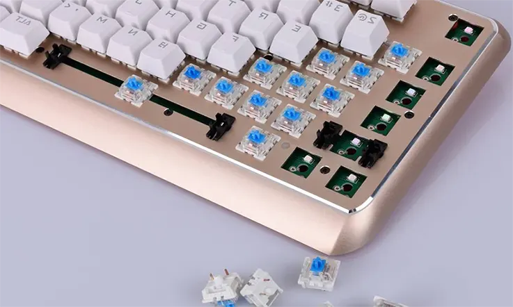
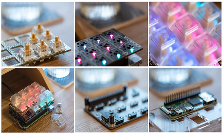
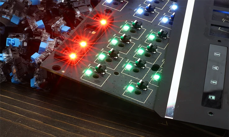
Mechanical keyboards offer a range of advantages over traditional keyboards, making them highly favored by many users. These keyboards are known for their exceptional tactile feedback, enhanced durability, and increased versatility. These benefits can be attributed, in part, to the utilization of printed circuit boards (PCBs) as the central components that connect various elements of the keyboard, including key switches, LEDs, diodes, and microcontrollers.
For keyboard enthusiasts, the process of designing a custom mechanical keyboard is an engaging and rewarding experience. By customizing the layout of the keyboard PCB to match individual preferences, one can create a unique and personalized keyboard that aligns with their specific needs and aesthetic preferences. In this informative article, Jarnis Technology will provide a comprehensive tutorial on the manufacturing process of mechanical keyboards, beginning with the essential steps involved in designing the PCB.
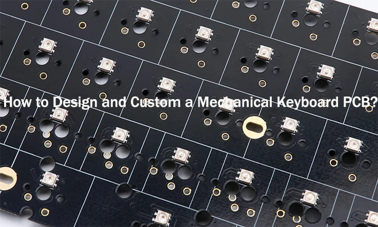
What is Mechanical Keyboard PCB?
A Mechanical Keyboard PCB (Printed Circuit Board) refers to the electronic component that serves as the foundation or backbone of a mechanical keyboard. It is a flat board made of insulating material, typically fiberglass, with a series of conductive pathways etched or printed onto its surface. The PCB acts as a platform for mounting and connecting various components of the keyboard, including switches, diodes, LEDs, and the controller.
The primary function of a mechanical keyboard PCB is to facilitate the electrical connections between the key switches and the keyboard’s controller. Each switch on the mechanical keyboard is soldered onto the PCB, and the conductive traces on the board carry the electrical signals from the switches to the controller. The PCB also provides a means for the controller to communicate with the computer or device it is connected to.
Additionally, the mechanical keyboard PCB may incorporate other features such as backlighting support, programmability, and various layout options. It plays a crucial role in determining the overall functionality, compatibility, and customization possibilities of the mechanical keyboard.
As a result, a mechanical keyboard PCB is the circuit board that enables the electrical connections between the switches and the controller, allowing for the input of keystrokes and the transmission of data to the computer or device.
Mechanical Keyboard PCB Design Features and Considerations
Mechanical keyboard PCB design involves the process of creating and optimizing the layout and circuitry of the PCB specifically tailored for a mechanical keyboard. Here are some key aspects and considerations involved in mechanical keyboard PCB design:
Key Layout and Matrix: Designing the PCB layout starts with determining the key matrix, which defines the arrangement and organization of the switches on the board. The matrix layout affects the electrical connections and determines the key rollover capabilities of the keyboard.
Switch Compatibility and Soldering: The PCB design should be compatible with the specific switches intended for use in the mechanical keyboard. This includes ensuring the correct footprint and pin layout for the switches. Proper soldering pads or through-hole vias must be designed to securely mount and solder each switch onto the PCB.
PCB Size and Form Factor: The physical dimensions and form factor of the PCB are crucial considerations in mechanical keyboard design. The PCB size should align with the desired keyboard size, whether it’s a full-size, tenkeyless (TKL), compact, or custom form factor.
Traces and Signal Routing: The PCB traces are the conductive pathways that carry electrical signals between the switches and the controller. Proper signal routing is essential to minimize electrical interference and ensure reliable key detection. Techniques such as trace width optimization, signal isolation, and ground plane design may be employed to enhance signal integrity.
PCB Features and Components: The PCB design may incorporate additional features, such as backlighting support for RGB LEDs or single-color LEDs. These features require appropriate circuitry and components on the PCB to control and power the lighting elements. Other components like diodes, resistors, and capacitors may also be included to support keyboard functionality.
USB Connectivity and Controller Options: The PCB design should include USB connectivity to establish a connection with the computer or device. The choice of the controller chip and its integration on the PCB is crucial for keyboard functionality, programmability, and firmware support.
Mounting and Stabilizer Support: The PCB design should consider the mounting mechanism for the PCB within the keyboard case. It should provide appropriate mounting holes or standoffs to secure the PCB. Additionally, if the keyboard uses stabilizers for larger keys, the PCB design should accommodate the stabilizer mechanism.
ESD Protection and EMI Considerations: Electrostatic discharge (ESD) protection measures and electromagnetic interference (EMI) considerations should be incorporated into the PCB design to ensure the keyboard’s reliability and compliance with regulatory standards.
Prototyping and Testing: Once the PCB design is complete, it is typically prototyped and tested to verify its functionality, key detection, and stability. Iterative testing and refinement may be necessary to address any issues or optimize the design further.
It’s worth noting that mechanical keyboard PCB design can range from simple DIY designs to complex custom designs, depending on the desired features, level of customization, and intended use of the keyboard.
What to do Before Designing a Mechanical keyboard PCB?
Budget
When embarking on a project, it is crucial to give careful consideration to the budgetary aspects, as they significantly influence the selection of components and the overall complexity of the design. As a distinguished PCBA company, JarnisTech offers valuable guidelines for effectively budgeting your project:
Establish a comprehensive budget: Commence the project by setting a realistic and well-defined budget, taking into account the anticipated costs associated with components and customization options. This initial step ensures that financial resources are allocated appropriately throughout the project lifecycle.
Conduct thorough research on component costs: Undertake extensive research to ascertain the costs of various components required for your project. It is advisable to explore reputable deals sites and avail yourself of any available discounts or promotions. By doing so, you can effectively manage expenses and potentially realize cost savings. JarnisTech provides exceptional component procurement services, guaranteeing the acquisition of genuine products at competitive prices.
Determine component priorities: Evaluate the functionalities of the components involved, differentiating between essential and optional features. This assessment allows you to prioritize the PCB design and allocate resources accordingly. For instance, if tactile feedback is a primary concern, it is prudent to invest more in high-quality key switches to enhance the overall user experience.
By adhering to these professional tips, you can ensure a meticulous budgeting process for your project, enabling you to make informed decisions regarding component selection and design complexity. JarnisTech stands ready to support you with our expertise in PCBA services, facilitating the successful realization of your project objectives while optimizing cost-efficiency.
Tools and Materials
Prior to commencing the process of custom keyboard PCB design, it is imperative to ensure that you possess the essential tools and materials. These encompass:
PCB design software: Utilize industry-standard tools such as Eagle, KiCad, or Altium to facilitate the creation of your custom keyboard PCB design.
Computer with USB port: Ensure that your computer is equipped with a functional USB port to establish connectivity with the custom keyboard PCB.
Microcontroller: Select a suitable microcontroller for your custom keyboard PCB, such as Atmega32u4 or STM32, which will serve as the central processing unit for the keyboard’s functionality.
Key switches: Acquire the desired key switches for your custom keyboard, such as Cherry MX or Kailh switches, which determine the tactile feel and responsiveness of the keys.
Diodes: Obtain an adequate number of diodes, with one diode required for each key switch. Diodes are necessary to prevent ghosting or key matrix issues.
Resistors: If your custom keyboard design incorporates LEDs, procure resistors to appropriately control the current flow to the LEDs, ensuring optimal performance and longevity.
Capacitor: Include a capacitor in your custom keyboard PCB design to stabilize the power supply, minimizing voltage fluctuations and potential interference.
LEDs: If your design incorporates backlighting or indicator lights, acquire suitable LEDs to fulfill the desired lighting requirements.
Soldering iron and solder: Possess a reliable soldering iron and high-quality solder to securely and effectively join the components and connections on the custom keyboard PCB.
Multimeter: Employ a multimeter, a versatile testing instrument, to assess the continuity and integrity of connections, enabling you to identify and rectify any potential issues.
By ensuring the availability of these tools and materials, you will be adequately equipped to embark on the custom keyboard PCB design process, thereby facilitating a smooth and successful implementation of your design vision.
How to Choosing the Right Mechanical Keyboard Components ?
Microcontroller Selection
When determining the requirements for your keyboard, there are several factors to consider in selecting an appropriate microcontroller:
Number of Keys: It is essential to determine the number of keys your keyboard will have. This information is crucial for ensuring that the microcontroller you choose has an adequate number of input/output (I/O) pins to connect all the keys effectively.
Communication Protocol: Verify that the microcontroller supports the desired communication protocol, such as USB or Bluetooth, which you intend to use for connecting the keyboard to the computer or other devices. This compatibility ensures seamless integration and reliable data transmission.
Processing Power: Evaluate the processing power of the microcontroller to ensure it can handle the specific features you plan to incorporate into your keyboard, such as RGB lighting effects or a display. Sufficient processing capabilities will enable these features to function smoothly without compromising the overall performance of the keyboard.
Availability and Cost: Choose a microcontroller that is readily available in the market and fits within your budget. Popular microcontrollers for mechanical keyboards include the Atmel AVR, PIC, and STM32 series. By opting for commonly used microcontrollers, you can benefit from the availability of resources, support, and cost-effective options.
Community Support: Consider selecting a microcontroller that has an active community of developers and users. This aspect contributes to a thriving ecosystem where you can find ample resources, documentation, and assistance with programming and troubleshooting. The presence of a supportive community greatly simplifies development and enhances the overall experience of working with the microcontroller.
By carefully considering these factors, you can choose a suitable microcontroller for your keyboard project that meets your requirements in terms of key count, communication protocol, processing power, availability, cost, and community support.
Key Switch Selection
Keyswitches are mechanical switches specifically designed to register keystrokes. Each type of keyswitch possesses unique characteristics that should be considered when making a selection. Key factors to focus on include tactile feedback, actuation force, and noise level. Presented below are four distinct types of keys:
Linear: Linear keys offer a seamless keystroke experience devoid of noticeable tactile bumps or audible feedback. These keys require lighter keystrokes to activate and are exemplified by switches like the Cherry MX Red.
Tactile: Tactile keys are characterized by a discernible bump when engaged, providing a clear tactile feedback sensation. They necessitate a specific degree of key force to activate, making them well-suited for precise typing. An example of a tactile keyswitch is the Cherry MX Brown.
Clicky: Clicky keys feature both tactile bumps and audible clicks, delivering physical and auditory feedback upon activation. These switches are known for their distinct click sound and tactile response. The Cherry MX Blue is a prominent example of a clicky keyswitch.
Silent: Silent keys incorporate noise suppression design elements to offer a quieter typing experience. These switches are engineered to minimize the noise generated during keystrokes while maintaining functionality. The Cherry MX Silent Red is an excellent illustration of a silent keyswitch.
When making a decision, it is important to consider the desired tactile feedback, actuation force, and noise level to ensure an optimal typing experience that aligns with individual preferences.
Diode-resistor-capacitor Selection
Diodes play a pivotal role in ensuring the optimal functionality of a mechanical keyboard PCB. They serve to prevent undesirable issues such as ghosting and key chatter by guaranteeing that only one keystroke is registered at a given time. Therefore, it is crucial to select the appropriate diodes in order to maintain compatibility with the PCB layout and key switches employed. Among the popular diode options available, the 1N4148 and 1N4148W stand out.
While not indispensable, the inclusion of resistors and capacitors can greatly contribute to the stability of the power supply and the reduction of noise in the keyboard PCB. Moreover, if the intention is to incorporate LEDs into the keyboard, resistors become essential to regulate the current flow through the LEDs and prevent any undesirable consequences.
LED Selection
LEDs have gained popularity as a sought-after addition to custom keyboards due to their ability to enhance the visual appeal and provide visual feedback. These LEDs can be utilized to backlight specific keys or introduce RGB lighting to the entire keyboard, offering a vibrant and customizable lighting experience. However, when selecting LEDs for such purposes, careful consideration of their power consumption becomes crucial.
It is noteworthy that RGB LEDs typically consume more power compared to their monochromatic counterparts. Consequently, it is advisable to choose LEDs that consume a reasonable amount of power to ensure the stable functioning of the power supply. This precautionary measure helps prevent any potential issues that may arise from power supply instability, thus ensuring a reliable and uninterrupted operation of the keyboard’s lighting system.
How to Make a Custom keyboard PCB?
Making a custom keyboard PCB (Printed Circuit Board) requires some knowledge of electronics and PCB design. Here are the general steps involved in creating a custom keyboard PCB:
Research and Planning
Determine the size and layout of your custom keyboard. Decide on the number and arrangement of keys, as well as any additional features like backlighting or programmability.
Research existing keyboard PCB designs and layouts to get an idea of what’s possible and to gather inspiration.
Schematic Design
Create a schematic diagram of your keyboard PCB using electronic design software like KiCad, Eagle, or Altium Designer.
Place the key switches, diodes (if using a matrix layout), microcontroller, and other components on the schematic.
Connect the components together, ensuring proper electrical connections.
PCB Layout Design
Once the schematic is complete, transfer the components to the PCB layout view in your design software.
Position the components on the PCB, taking care to consider key placement, switch spacing, and any additional features.
Route the electrical traces between the components, ensuring proper connections and avoiding any interference or short circuits.
Pay attention to signal integrity, ground planes, and power distribution.
Design Rule Check (DRC)
Run a Design Rule Check in your PCB design software to verify that your design meets the manufacturing requirements and constraints.
Fix any errors or warnings identified by the DRC to ensure the PCB is manufacturable.
Output Generation
Generate the necessary output files for manufacturing the PCB, such as Gerber files, drill files, and any additional manufacturing files required by your chosen PCB manufacturer.
Prototype Manufacturing
Send the generated files to a PCB manufacturer or fabricate the PCB yourself if you have the necessary equipment.
Choose a manufacturer that suits your requirements in terms of quality, cost, and turnaround time.
Review and approve the manufacturer’s design for manufacturing (DFM) feedback if provided.
Assembly and Testing
Once you receive the manufactured PCB, source the necessary components like key switches, diodes, microcontroller, and other electronic parts.
Solder the components onto the PCB following proper soldering techniques.
Connect the keyboard PCB to a computer and test the functionality of each key, ensuring proper electrical connections and programming if applicable.
Note: Designing a custom keyboard PCB requires knowledge of electronics, PCB design software, and soldering techniques. It’s recommended to have prior experience or seek guidance from knowledgeable individuals or communities specializing in keyboard design.
How to DIY a mechanical keyboard ?
Building a mechanical keyboard yourself can be a rewarding DIY project. Here’s a general guide to help you get started:
1. Gather Components:
Mechanical switches: Choose the type of switches you prefer, such as Cherry MX, Gateron, Kailh, etc. Consider factors like tactile feedback, actuation force, and noise level.
Keycaps: Select keycaps that fit your chosen switches. There are various materials, profiles, and designs available.
PCB (Printed Circuit Board): You can either design and manufacture a custom PCB as discussed in the previous response or purchase a pre-made PCB that fits your desired layout.
Controller: Obtain a microcontroller or controller board that will serve as the brain of your keyboard. Popular choices include Arduino Pro Micro, Teensy, or custom-designed PCBs with integrated controllers.
Stabilizers: If your keyboard layout includes larger keys like spacebar or shift keys, you’ll need stabilizers to ensure smooth key movement. Cherry-style or screw-in stabilizers are commonly used.
Case: Decide whether you want a custom-made case or if you’ll repurpose an existing keyboard case. Consider factors like material, design, and compatibility with your chosen components.
Other components: You may need soldering equipment (soldering iron, solder wire), wire, diodes (if not integrated into the PCB), and mounting screws.
2. Prepare the PCB:
If you’re using a pre-made PCB, ensure it’s compatible with your chosen switches and key layout.
If you’re designing your own PCB, follow the steps outlined in the previous response to create the schematic, PCB layout, and generate manufacturing files.
If necessary, solder any additional components like diodes onto the PCB.
3. Soldering:
Place the switches into their designated positions on the PCB.
Heat up your soldering iron and apply a small amount of solder to the tip.
Heat the switch’s solder pad and the corresponding pin, and then apply solder to create a secure connection.
Repeat this process for all the switches on the PCB.
If your PCB has through-hole components like LEDs or resistors, solder them as well.
4. Install Stabilizers:
If your keyboard layout includes larger keys, you’ll need to install stabilizers for smooth key movement.
Insert the stabilizers into the designated positions on the PCB or case.
Attach the stabilizer wire to the stabilized keys (spacebar, shift keys) as per the manufacturer’s instructions.
5. Mount the PCB:
Place the PCB into the case, ensuring it fits securely and aligns with the mounting holes.
Use the provided mounting screws or other fastening methods to secure the PCB to the case.
6. Install Keycaps:
Take your chosen keycaps and press them firmly onto the switches, ensuring they are aligned and seated properly.
7. Testing:
Connect the keyboard to a computer using a USB cable.
Test each key to verify that it registers correctly.
f necessary, program the keyboard’s firmware using software like QMK or VIA to customize key mappings, lighting effects, and other features.
8. Final Assembly:
Once you’re satisfied with the functionality and aesthetics, reassemble the case if it was disassembled during the process.
Double-check all connections and ensure everything is securely in place.
That’s it! You have successfully DIYed your mechanical keyboard. Enjoy typing on your custom creation!
Why Choose JarnisTech for Your Mechanical Keyboard PCB ?
If you are seeking a reputable supplier for professional mechanical keyboard PCBs in China, JarnisTech is the optimal choice for you. Equipped with a sizable workshop housing more than 500 skilled workers, we boast a substantial monthly production capacity of 40,000 square meters.
At JarnisTech, our production department operates on two to three shifts, ensuring that even during peak seasons, your delivery timeline remains unaffected. We prioritize maintaining prompt delivery schedules to meet your requirements.
As a trusted mechanical keyboard PCB supplier, JarnisTech prides itself on an engineering team with over 20 years of design experience. Our expertise has been leveraged by a diverse clientele of 3000+ customers worldwide, spanning countries such as the USA, Canada, Germany, UK, Spain, Italy, Sweden, Norway, and more.
When you embark on designing a new mechanical keyboard and require a prototype PCB within a tight 24-hour timeframe, JarnisTech is well-equipped to assist you promptly.
Rest assured that our sales team is attuned to your working hours, enabling them to promptly respond to your emails or inquiries, eliminating concerns regarding time differences.
Once you are prepared to proceed with your mechanical keyboard PCB order, kindly forward your CAD file or Gerber file to us. Our proficient engineering team will meticulously review the files prior to commencing manufacturing.
We encourage you to submit your quote to us without delay, and we assure you that we will promptly furnish you with a comprehensive quotation.
In Conclusion
Mechanical Keyboard PCBs play a crucial role in the performance and functionality of mechanical keyboards. Their design, compatibility, and quality are essential factors that directly impact the overall user experience. As technology continues to evolve, we can expect further innovation and customization options in the realm of Mechanical Keyboard PCBs. Whether you’re a casual user or an avid keyboard enthusiast, understanding the intricacies of PCBs in mechanical keyboards can help you make informed decisions when selecting or designing your own keyboard.
As a PCB designer, one often encounters the intricate nature of circuit design and occasionally wishes for a software solution that could simplify the process while reducing shipment time. Well, the wish has now become a reality with ExpressPCB.
ExpressPCB empowers PCB designers to effortlessly create schematic designs and generate PCB layouts. What sets it apart is its remarkable shipping speed, with a minimum turnaround time of five days, whereas other providers may take anywhere from 10 to 15 days. This impressive reduction in shipment time is complemented by a software that streamlines complexity, resulting in cost savings as well.
In this comprehensive guide, we will delve into the fundamentals of ExpressPCB, including an introduction to the software and a step-by-step tutorial on how to export Gerber files. Additionally, we will provide valuable insights from ExpressPCB users who have shared their experiences with the platform.
Prepare to embark on a journey through the world of ExpressPCB, where complexity is simplified, shipment time is minimized, and costs are optimized. Let us now proceed with the guide, unlocking the potential of this remarkable software.
Introduction to Express PCB
Express PCB is a software tool used for designing printed circuit boards (PCBs). It provides a user-friendly interface and a streamlined workflow, making it suitable for beginners and hobbyists who are new to PCB design. With Express PCB, you can create schematics, place components, route traces, and generate manufacturing files necessary for PCB fabrication.
Express PCB is known for its simplicity and ease of use. It offers a straightforward approach to PCB design without overwhelming users with complex features and options. This makes it a popular choice for quick prototyping, small projects, and educational purposes.
Benefits and Features of Express PCB:
User-Friendly Interface: Express PCB features a simple and intuitive interface that makes it easy to navigate and understand. The toolbar, menus, and project explorer are designed to provide quick access to essential functions and components.
Rapid Prototyping: With Express PCB, you can quickly transform your circuit ideas into physical PCB designs. Its streamlined workflow allows for faster iterations and prototyping, reducing the time required to bring your projects to life.
Component Library: Express PCB includes a built-in library of commonly used components, such as resistors, capacitors, ICs, connectors, and more. This library simplifies the process of selecting and placing components on the board, saving you time and effort.
Design Rule Checking (DRC): Express PCB performs automatic design rule checks to ensure that your PCB design meets specific manufacturing constraints and specifications. It helps identify potential errors or violations early in the design process, allowing you to make necessary adjustments.
Gerber File Generation: Express PCB can generate Gerber files, which are the standard file format used by PCB manufacturers to fabricate PCBs. These files contain all the necessary information about the PCB layers, traces, pads, and holes.
Cost-Effective: Express PCB offers a free version of its software, allowing users to create simple PCB designs without any licensing costs. This makes it an attractive option for hobbyists and those on a tight budget.
Overview of the PCB Design Process:
The PCB design process typically involves the following steps:
1. Schematic Design: Create a schematic diagram of your circuit, defining the connections between various components and their electrical relationships.
2. Component Placement: Place the components on the PCB layout, considering factors such as component clearance, signal integrity, and thermal considerations.
3. Routing: Connect the components through traces, carefully routing signals to avoid interference and maintain proper signal integrity.
4. Design Rule Checking: Run a design rule check to ensure that your design meets manufacturing constraints, such as minimum trace width, spacing, and clearance requirements.
5. Gerber File Generation: Generate the necessary manufacturing files, including Gerber files, drill files, and assembly files, to communicate your design specifications to the PCB manufacturer.
6. PCB Fabrication: Send the generated files to a PCB manufacturer for fabrication. The manufacturer will use these files to produce the physical PCBs based on your design.
Express PCB simplifies these steps by providing a user-friendly interface and automating certain aspects of the design process, allowing you to focus on the core aspects of your PCB design.
In the following sections, we will delve deeper into each aspect of using Express PCB, from installation and project setup to component placement, routing, and generating manufacturing files.
Installing Express PCB
Installing Express PCB is a straightforward process. Here is a step-by-step guide to help you install Express PCB on your computer:
System Requirements
Before you begin the installation, make sure your computer meets the minimum system requirements for running Express PCB. These requirements may vary depending on the version of Express PCB you are installing. Check the official documentation or the system requirements provided by Express PCB for the specific version you are using.
Downloading the Software
Visit the Express PCB website or the official download page to obtain the installation package. Look for the appropriate version of Express PCB that matches your operating system (Windows) and download the installer file to your computer.
Running the Installer
Locate the downloaded installer file on your computer and double-click on it to run the installation wizard. If prompted by the operating system’s security features, confirm that you want to proceed with the installation.
Accepting the License Agreement
The installation process begins with displaying the End-User License Agreement (EULA). Read through the agreement carefully and if you agree to the terms, click on the “I accept the agreement” or similar button to proceed with the installation.
Choosing the Installation Location
The installer will present you with the option to choose the installation location for Express PCB. You can either accept the default location or select a different directory where you want the software to be installed. Once you have made your selection, click on the “Next” or “Install” button to continue.
Selecting Additional Components (if applicable)
Depending on the version of Express PCB you are installing, you may be given the option to choose additional components or features to be installed along with the main software. Select the desired options, or if there are no additional components, skip this step by clicking on the “Next” or “Install” button.
Installing
The installer will now proceed to install Express PCB on your computer. It may take a few moments to complete the installation process. You may see a progress bar or indicator showing the installation progress.
Completing the Installation
Once the installation is finished, you will see a completion message or prompt indicating that Express PCB has been successfully installed on your computer. At this point, you may be given the option to launch the software immediately. If not, you can close the installer.
Launching Express PCB
To start using Express PCB, locate the software’s shortcut icon on your desktop or in the Start menu. Double-click on the icon to launch the application.
Activation and Licensing (if required)
Depending on the version of Express PCB you are using, you may need to activate and license the software. Follow the instructions provided by Express PCB to activate your copy of the software. This usually involves entering a license key or registering your account.
That’s it! You have now successfully installed Express PCB on your computer. You can now start exploring the software and begin creating your PCB designs.
Navigating the User Interface
Navigating the user interface of Express PCB involves understanding the layout, toolbars, menus, project explorer, library browser, and customization options. Here’s a breakdown of the key components:
Main Window Layout
The main window of Express PCB consists of various sections. It typically includes a workspace where you design your PCB layout, menus and toolbars for accessing different features and functions, and panels for displaying information, such as the project explorer and library browser.
Toolbars and Menus
Express PCB provides toolbars and menus to access various commands and functions. The toolbars typically contain icons representing common operations like opening, saving, zooming, placing components, routing traces, etc. The menus offer more comprehensive access to functions categorized under different menu items, such as File, Edit, View, Tools, and Help.
Project Explorer
The project explorer is a panel that displays the hierarchy of your project. It shows the project name, folder structure, and files associated with the project. You can use it to organize your project files and easily switch between different design files.
Library Browser
The library browser allows you to manage and access component libraries. It displays a list of available libraries and their contents. You can browse through the libraries, search for specific components, and add them to your project.
Setting Preferences and Customization Options
Express PCB provides options to customize the user interface and configure various settings to suit your preferences. You can access these options through the Preferences or Settings menu. Here, you can adjust settings related to units, grid spacing, colors, shortcuts, and more.
It’s important to spend some time familiarizing yourself with the user interface of Express PCB by exploring the different sections, menus, and toolbars. This will help you navigate efficiently and access the necessary functions for designing your PCB layout.
Creating a New PCB Project
Creating a new PCB project in Express PCB involves a few steps to set up the project parameters, define the board size and layers, and manage the components and libraries. Here’s a guide to creating a new PCB project:
Launch Express PCB
Start by launching the Express PCB software on your computer. Ensure that you have installed the software correctly.
Start a New Project
In the main menu, go to “File” and select “New” or use the corresponding toolbar icon to start a new project. This will open a blank project window.
Configure Project Parameters
In the project window, go to the “Project” menu or toolbar and select “Project Options” or “Properties.” Here, you can configure various project parameters such as the project name, description, author, revision, and date. Fill in the necessary details for your project.
Define Board Size and Layers
In the project window, go to the “Project” menu or toolbar and select “Board Layout.” This will open the PCB layout editor. In the editor, define the board size by specifying the width and height of the PCB. You can also set the number of layers you want to use for your design. Adjust these parameters according to your requirements.
Manage Components and Libraries
To manage components and libraries, go to the “Library” menu or toolbar and select “Component Manager” or “Library Manager.” In the component manager, you can add, remove, or edit components for your project. You can also create custom components or import components from existing libraries. In the library manager, you can manage your component libraries, add new libraries, and specify the location of your library files.
Save the Project
Once you have set up the project parameters, board size, and component libraries, it’s essential to save your project. Go to the “File” menu and select “Save” or use the save toolbar icon. Choose a location on your computer and provide a name for your project file. Saving the project file ensures that your progress is saved and can be easily accessed in the future.
You have now created a new PCB project in Express PCB. You can start designing your PCB layout by placing components, routing traces, and configuring other design elements. Remember to save your work regularly to avoid any data loss.
Designing the PCB Layout
Designing the PCB layout is a crucial step in the PCB design process. Express PCB offers a range of tools and features to help you create an efficient and functional layout. Here are the key steps involved in designing the PCB layout:
Placing Components on the Board:
Start by placing the components on the board. You can either select components from the built-in library or create custom components if necessary. Use the drag-and-drop functionality to position the components in the desired locations on the board.
Connecting Traces and Routing:
Once the components are placed, you need to establish connections between them by routing traces. Use the routing tools provided by Express PCB to draw traces between the component pins. Ensure that you follow design rules and guidelines to maintain signal integrity and avoid interference.
Adding Vias, Pads, and Through-Hole Components:
Depending on your design requirements, you may need to add vias, pads, and through-hole components. Vias allow you to create connections between different layers of the PCB. Pads are used to create landing areas for surface-mounted components, while through-hole components require holes to accommodate their leads.
Defining Power and Ground Planes:
To ensure proper power distribution and minimize noise, it’s often beneficial to include power and ground planes in your PCB design. Express PCB provides tools to define these planes and establish connections to power and ground pins of the components. This helps in creating a solid reference for signal integrity and reducing electromagnetic interference.
Design Rule Checking (DRC):
After completing the layout, it’s essential to run a design rule check (DRC) to validate your design against predefined rules and constraints. Express PCB’s DRC feature examines your layout for potential errors, such as incorrect clearances, overlapping traces, or missing connections. Address any issues identified by the DRC to ensure a manufacturable and functional PCB design.
Throughout the design process, it’s important to consider best practices such as component placement strategies, signal integrity, and manufacturability. Efficient component placement minimizes signal interference and facilitates routing. Proper trace routing techniques, such as using differential pairs and avoiding sharp angles, help maintain signal integrity. Additionally, following design guidelines for manufacturability ensures that your design can be fabricated and assembled without issues.
Express PCB provides a user-friendly interface and a set of tools to simplify the PCB layout process. Take advantage of these features, and don’t hesitate to consult the software’s documentation or online resources for more detailed instructions on specific functions.
Generating Manufacturing Files
Generating manufacturing files in Express PCB involves creating the necessary files that are required by PCB manufacturers to fabricate your design. The most common manufacturing files include Gerber files and the Bill of Materials (BOM). Here’s an overview of the process:
Gerber File Generation:
Gerber files are the standard format used to describe the different layers of your PCB design. They contain information about copper traces, solder masks, silk screens, drill holes, and other relevant features. To generate Gerber files in Express PCB, follow these steps:
a. Open your PCB design in Express PCB.
b. Go to the File menu and select “Export”.
c. Choose the option for Gerber files or Gerber 274X.
d. Specify the output folder and file names for each Gerber layer.
e. Select the desired layers to include in the Gerber files, such as top copper, bottom copper, solder mask, silk screen, etc.
f. Adjust any additional settings or options as required.
g. Click on the “Export” or “Generate” button to create the Gerber files.
Once generated, you can provide the Gerber files to your PCB manufacturer for fabrication.
Bill of Materials (BOM) Generation:
The Bill of Materials (BOM) is a document that lists all the components used in your PCB design, along with their quantities and reference designators. It helps the manufacturer identify and source the required components. To generate a BOM in Express PCB, follow these steps:
a. Open your PCB design in Express PCB.
b. Go to the File menu and select “Export”.
c. Choose the option for Bill of Materials (BOM).
d. Specify the output file name and location.
e. Adjust any additional settings or options, such as including attributes like part numbers or descriptions.
f. Click on the “Export” or “Generate” button to create the BOM file.
The generated BOM file can be provided to the manufacturer along with the Gerber files.
It’s important to note that the specific steps and options for generating manufacturing files may vary slightly depending on the version of Express PCB you are using. It’s recommended to refer to the software’s documentation or help resources for detailed instructions tailored to your version. Additionally, it’s always a good idea to communicate with your PCB manufacturer to ensure you provide them with the correct files and any additional requirements they may have.
Tips and Best Practices
Here are some tips and best practices to consider when working with Express PCB or any PCB design software:
Plan your design: Before diving into the PCB layout, spend time planning your design. Consider the components, their placement, power and ground connections, signal routing requirements, and any design constraints. Planning ahead will help you avoid mistakes and make the layout process smoother.
Component placement: Place components strategically to optimize signal integrity, minimize trace lengths, and ensure proper heat dissipation. Group related components together and place critical components first. Consider factors like component height, clearance, and accessibility for assembly and maintenance.
Trace routing: Follow good routing practices to minimize noise, crosstalk, and signal integrity issues. Use appropriate trace widths based on current requirements and impedance control. Keep traces as short and direct as possible and avoid sharp angles. Use ground and power planes whenever possible.
Design rule checking (DRC): Run the DRC feature to check for errors and rule violations. This helps ensure that your design meets the fabrication and assembly requirements. Pay attention to DRC warnings and resolve them to improve the overall quality of your design.
Use design layers effectively: Utilize different layers available in Express PCB to separate different types of signals, power and ground planes, and component outlines. This improves readability, simplifies debugging, and optimizes the PCB layout.
Document your design: Properly annotate and document your design to provide clear information to yourself and others involved in the project. Add reference designators, component values, and other necessary information to the PCB layout.
Test and verify: Before sending your design for fabrication, perform a thorough review and testing. Use the built-in simulation and analysis tools if available. Double-check component footprints, net connections, and design specifications to minimize the risk of errors.
Collaboration and version control: If you’re working in a team, establish a collaboration and version control system to manage design iterations, track changes, and avoid conflicts. This ensures smooth collaboration and prevents accidental overwriting or loss of work.
Seek community and online resources: Join PCB design forums, communities, or online platforms to connect with other designers, share knowledge, and seek advice. Many resources, tutorials, and design guidelines are available online to supplement your learning and help you overcome challenges.
Stay updated: Keep up with the latest updates, bug fixes, and new features released for Express PCB or any PCB design software you’re using. Regularly update your software to benefit from improvements and ensure compatibility with the latest industry standards.
Remember, practice and experience are key to becoming proficient in PCB design. Don’t be afraid to experiment, learn from mistakes, and continuously improve your skills.
Troubleshooting and Support
When working with Express PCB or encountering issues during the PCB design process, here are some troubleshooting tips and support options to consider:
Documentation and User Guides: Start by reviewing the official documentation and user guides provided by Express PCB. These resources often contain troubleshooting sections that address common issues and provide solutions.
Online Forums and Communities: Join online forums and communities dedicated to PCB design, such as the Express PCB user forum or general electronics design communities. Post your questions or search for existing threads related to your issue. Often, experienced users or even Express PCB representatives can provide guidance and solutions.
Knowledge Base and FAQs: Check the Express PCB website for a knowledge base or a frequently asked questions (FAQ) section. They often contain answers to common queries and troubleshooting steps for known issues.
Customer Support: If you’re unable to find a solution through online resources, reach out to Express PCB’s customer support. They can provide assistance and guidance for resolving specific issues related to their software. Contact information for customer support is typically available on the Express PCB website.
Software Updates: Ensure that you have the latest version of Express PCB installed. Software updates often include bug fixes and improvements that can address known issues. Check for updates regularly and install them as necessary.
Error Messages and Logs: Pay attention to any error messages or warnings generated by the software. These messages can provide valuable information about the cause of the issue. Take note of the specific error message or code and include it when seeking assistance. Additionally, check log files or error logs generated by Express PCB for additional details.
Double-Check Design Rules: If you’re encountering issues during the design or manufacturing file generation process, review your design rules. Ensure that your design adheres to the specified rules and constraints, such as trace widths, clearances, and component placement rules. Adjusting or relaxing certain design rules might resolve issues.
Hardware Compatibility: Check that your computer system meets the minimum requirements specified by Express PCB. Inadequate hardware resources can lead to software performance issues or instability. Verify that your operating system, processor, memory, and graphics capabilities are compatible with the software.
Reinstall or Repair: If you’re experiencing persistent issues that are not resolved through other troubleshooting steps, consider reinstalling or repairing the Express PCB software. This can help resolve any corrupted or missing files that might be causing the problem. Follow the instructions provided by Express PCB for reinstalling or repairing the software.
Remember to provide clear and detailed information when seeking support or troubleshooting assistance. Include relevant error messages, steps to reproduce the issue, and any specific circumstances surrounding the problem. This will help support personnel or community members better understand your situation and provide accurate guidance.
A Reliable Express PCB Manufacturing Service:JarnisTech
JarnisTech is dedicated to providing hobbyists and engineers worldwide with top-notch Quick Turn PCBs at competitive prices. Our expedited service ensures a swift turnaround time of just 24 hours, allowing you to meet tight project deadlines. To take advantage of our same day quick turnaround service, kindly ensure that your files are submitted before 9am. For further details regarding this service, we encourage you to reach out to us directly.
Engineers rely on JarnisTech due to our exceptional track record of delivering orders punctually and our commitment to manufacturing excellence. By opting for our accelerated service, you can significantly reduce the standard lead time of 2 weeks, enabling quicker prototyping of your critical PCBs. With our cost-effective pricing and unwavering reliability, you can minimize the risk of subpar PCBs while maximizing the return on investment for your PCB prototyping endeavors with JarnisTech.
Final Thoughts
This article has provided an overview of getting started with Express PCB, a popular software tool for designing printed circuit boards. We discussed the installation process, navigating the user interface, creating a new PCB project, designing the layout, performing design rule checks, generating manufacturing files, and shared some tips and best practices.
To sum up, mastering PCB design takes time and practice. Be patient with yourself, learn from your mistakes, and strive for continuous improvement. With dedication and a thirst for knowledge, you can become proficient in Express PCB and create high-quality PCB designs. Good luck on your PCB design journey!
The Micro Ball Grid Array (µBGA), also known as the Micro BGA or Micro Ball Grid Array, is widely regarded as one of the most cutting-edge and sophisticated surface-mounted devices available to PCB designers. It represents a specialized subset of the general Ball Grid Array (BGA) packaging technology. In a standard BGA package, the spacing between individual balls typically ranges from 0.8mm to 1.0mm, whereas the micro BGA package exhibits a much tighter pitch of 0.4mm or even less. This significant reduction in pitch allows for a considerable decrease in package size, enabling micro BGAs to be positioned in extremely close proximity to the PCB surface.
The packaging technology employed in electronic devices plays a crucial role in their overall performance. In recent years, advancements in technology have successfully minimized the signal delay within the actual semiconductor material of integrated circuits (ICs). However, the reduction of signal delay within the IC package itself remains limited. Consequently, the package becomes an integral component in facilitating high-speed performance in electronic devices. The micro BGA, with its superior chip delay capabilities, emerges as an ideal solution among various packaging technologies available. It offers greater flexibility and efficiency compared to alternative options, allowing for enhanced performance in high-speed applications.
Advantages and applications of µBGA
Here are some common advantages and applications of µBGA (micro ball grid array) technology:
Advantages of µBGA:
Miniaturization: The small size of µBGA packages allows for high circuit density and miniaturization of electronic devices.
Increased I/O Density: The µBGA design enables a higher number of input/output (I/O) connections within a smaller footprint.
Improved Electrical Performance: The shorter electrical path lengths and reduced parasitic capacitance and inductance in µBGA packages can enhance signal integrity and electrical performance.
Enhanced Thermal Performance: The small package size of µBGA facilitates efficient heat dissipation, leading to improved thermal management.
Cost-Effective Manufacturing: The automated assembly processes for µBGA packages result in higher production yields and lower manufacturing costs compared to larger packages like BGAs or quad flat packages (QFPs).
Applications of µBGA:
Consumer Electronics: µBGA technology finds extensive use in consumer electronic devices such as smartphones, tablets, wearables, gaming consoles, and digital cameras, where space-saving and high functionality are crucial.
IoT Devices:Internet of Things (IoT) devices, including smart home devices, connected sensors, and wearable devices, often employ µBGA packages due to their compact size and low power consumption.
Automotive Electronics: µBGA packages are utilized in automotive applications, including advanced driver-assistance systems (ADAS), infotainment systems, engine control units (ECUs), and in-vehicle networking, where space constraints and reliability are important.
Medical Devices: Medical equipment, such as portable monitors, implantable devices, and diagnostic tools, can benefit from µBGA technology to achieve small form factors and high-performance requirements.
Aerospace and Defense: The aerospace and defense industries utilize µBGA packages in applications like avionics systems, satellite communications, radar systems, and military-grade electronics, where size, weight, and reliability are critical factors.
These are just a few examples of the advantages and applications of µBGA technology. The specific advantages and applications may vary depending on the industry and the requirements of the electronic devices being developed.
Understanding BGA Technology
Understanding BGA (Ball Grid Array) technology is essential for anyone working with electronic components and circuit board design. BGA is a packaging technology that provides a reliable and compact solution for mounting integrated circuits (ICs) onto printed circuit boards (PCBs). Here are some key points to help you understand BGA technology:
1. Basic Concept: BGA is a surface-mount package where the IC is mounted directly onto the PCB. It uses an array of solder balls located on the bottom surface of the package to establish electrical connections between the IC and the PCB.
2. Advantages: BGA offers several advantages over other packaging technologies, such as:
● Higher I/O Density: BGA packages can accommodate a large number of input/output (I/O) connections, allowing for high-density circuit designs.
● Enhanced Electrical Performance: The short electrical path lengths and reduced parasitic inductance and capacitance of BGA packages can improve signal integrity and high-speed performance.
● Improved Thermal Performance: BGA packages have a larger thermal contact area with the PCB, enabling better heat dissipation, which is crucial for power-hungry ICs.
● Reduced PCB Space: BGA’s compact design allows for efficient use of PCB real estate, making it suitable for miniaturized devices.
● Higher Assembly Yield: BGA’s solder ball connections are less susceptible to mechanical stress during assembly, resulting in improved manufacturing yield rates.
3. Package Structure: A BGA package consists of several layers, including the substrate, die, solder balls, and underfill material. The substrate acts as a carrier for the IC, providing electrical and mechanical connections between the die and the PCB. The solder balls serve as the interface between the package and the PCB, forming the electrical connections.
4. Types of BGA: There are different types of BGA packages, including:
● PBGA (Plastic Ball Grid Array): PBGA packages are made of plastic and are commonly used in consumer electronics and low- to medium-density applications.
● CCGA (Ceramic Column Grid Array): CCGA packages utilize ceramic material, offering higher thermal conductivity and reliability, making them suitable for high-temperature and high-reliability applications.
● TBGA (Thin Ball Grid Array): TBGA packages have a thinner profile and are used when space constraints are critical, such as in mobile devices and ultra-thin laptops.
● Design Considerations: When working with BGA technology, certain design considerations are important, including:
● PCB Layout: Proper PCB layout is crucial for achieving optimal electrical and thermal performance. Specific guidelines, such as trace routing, via placement, and power/ground plane design, should be followed.
● Routing and Fanout: Careful routing and fanout techniques are necessary to distribute the I/O connections effectively and maintain signal integrity.
● Thermal Management: BGA packages generate heat, so thermal vias, heat sinks, and proper airflow should be considered to dissipate heat effectively and prevent overheating.
● Solder Joint Reliability: The reliability of solder joints is essential to ensure long-term functionality. Factors such as solder ball size, solder paste, reflow profile, and underfill material should be carefully selected and controlled.
Understanding BGA technology and its considerations is crucial for successful PCB design and manufacturing. Proper implementation of BGA packages can lead to improved performance, miniaturization, and reliability in electronic devices.
Key Components of µBGA
The key components of a µBGA (micro ball grid array) package include:
Substrate or PCB (Printed Circuit Board): The substrate serves as the foundation for the µBGA package, providing mechanical support and electrical interconnections. It is typically made of a laminate material with multiple layers of copper traces, vias, and pads.
Solder Balls: The solder balls are small spheres of solder alloy (typically lead-based or lead-free) that are attached to the bottom surface of the µBGA package. These solder balls serve as the electrical and mechanical connections between the package and the PCB. They are usually arranged in a grid pattern, forming the ball grid array.
Die/Chip: The die, also known as the chip, is the semiconductor component that contains the integrated circuits (ICs) or other active devices. The die is mounted onto the substrate and wire bonded or flip-chip bonded to establish electrical connections between the die and the substrate.
Underfill Material: The underfill material is a specialized epoxy resin that is injected or dispensed between the die and the substrate. It fills the space between the die and the substrate, encapsulating the wire bonds or solder bumps. The underfill material provides mechanical reinforcement, stress relief, and thermal conductivity, enhancing the reliability of the µBGA package.
It’s important to note that while these are the primary components of a µBGA package, there may be additional elements such as solder mask, solder resist, and protective coatings to provide insulation, protect against environmental factors, and improve reliability. The specific design and composition of these components may vary depending on the requirements of the application and the manufacturing processes used.
µBGA: Design Considerations
When designing with µBGA (micro ball grid array) technology, there are several important considerations to keep in mind. Here are some key design considerations:
1. Package Size and Density:
● Determine the appropriate package size based on the available board space and the desired circuit density.
● Consider the pitch (spacing) between the solder balls to ensure proper routing and manufacturability.
● Balance the need for miniaturization with the requirements for signal integrity, thermal management, and accessibility for testing or rework.
2. Thermal Management:
● Evaluate the thermal requirements of the components and the system to ensure efficient heat dissipation.
● Use appropriate thermal vias and conductive planes in the PCB layout to aid in heat transfer.
● Consider the use of thermal pads or heat sinks on the package to improve thermal performance.
3. Electrical Considerations:
● Pay attention to signal and power integrity to minimize noise and ensure reliable operation.
● Consider impedance control and signal termination techniques to maintain signal quality.
● Optimize power distribution and decoupling capacitor placement to minimize voltage drops and noise.
4. Signal Integrity and Routing Guidelines:
● Follow recommended routing guidelines provided by the manufacturer to maintain signal integrity.
● Minimize signal length and high-speed signal reflections by using controlled impedance traces and avoiding stubs.
● Avoid crossing sensitive high-speed signals with noisy or high-current traces to minimize crosstalk and interference.
5. Manufacturing and Assembly:
● Collaborate with the manufacturing team to ensure that the PCB design meets the assembly requirements for µBGA packages.
● Consider the solder mask and solder paste requirements, pad design, and stencil design for accurate and reliable assembly.
● Verify that the assembly process can accommodate the specific requirements of µBGA, such as ball placement accuracy and reflow temperatures.
6. Testing and Rework:
● Plan for testability during the design phase by including test points and access to critical signals.
● Consider the accessibility of the solder balls for rework or repair, if needed.
● Implement proper test and inspection methodologies to ensure the reliability of the assembled µBGA packages.
It’s essential to consult the datasheets, guidelines, and application notes provided by the specific manufacturer of the µBGA packages you are working with, as they may have additional design considerations and recommendations specific to their products. Additionally, working closely with experienced PCB designers and manufacturing engineers can help ensure a successful design implementation with µBGA technology.
µBGA: Manufacturing and Assembly
Manufacturing and assembly processes for µBGA (micro ball grid array) packages involve several steps to ensure proper placement, attachment, and quality control. Here are some key aspects of the manufacturing and assembly of µBGA packages:
1. PCB Layout Considerations:
● Design guidelines: Follow specific design guidelines provided by the package manufacturer to ensure proper layout and signal integrity.
● Trace routing: Pay attention to trace widths, spacing, and impedance control to maintain electrical performance.
● Thermal considerations: Incorporate thermal vias or thermal pads to aid in heat dissipation from the package.
2. Ball Attach and Reflow Process:
● Solder ball attachment: Precise placement of solder balls on the µBGA package using automated equipment, such as pick-and-place machines or specialized dispensing systems.
● Flux application: Apply a flux material to the solder pads on the PCB to promote proper wetting and solder joint formation.
● Reflow soldering: Subject the assembled PCB to a controlled heating process, typically using a reflow oven, to melt the solder balls and establish electrical and mechanical connections.
3. Inspection and Quality Control:
● X-ray inspection: Utilize X-ray equipment to verify proper ball alignment, solder joint quality, and detect any potential defects or voids.
● Automated optical inspection (AOI): Employ AOI systems to perform visual inspections of solder joints, component placement, and overall assembly quality.
● Electrical testing: Conduct electrical tests, such as continuity checks, functional testing, or in-circuit testing, to ensure proper electrical connectivity and functionality of the assembled µBGA packages.
4. Rework and Repair:
● Rework processes: Develop rework procedures to address any defective or improperly connected µBGA packages, including removal of faulty packages, cleaning of solder pads, and re-attachment of new packages.
● Repair techniques: Implement repair techniques, such as soldering or reflowing specific solder joints, to rectify any identified issues during inspection or testing.
It’s important to note that the specific manufacturing and assembly processes may vary depending on the production facility, equipment used, and specific requirements of the µBGA package and PCB design. Manufacturers often follow industry standards, guidelines from package suppliers, and their own internal quality control practices to ensure the reliable assembly of µBGA packages.
µBGA (Micro Ball Grid Array) Defect Inspection
After the soldering process, the detection of defects in Ball Grid Array (BGA) components becomes crucial. Various factors such as component quality, equipment functionality, soldering procedures, and environmental conditions can contribute to the occurrence of defects. These defects encompass issues like open circuits, cold soldering, short circuits, bridging, incomplete soldering, and misalignment. Additionally, problems may arise with the BGA solder balls themselves, such as missing balls and inconsistent sizes.
Inspecting BGAs poses challenges in ensuring the high quality of the final product. This is primarily due to the positioning of the solder balls beneath the visual inspection and the chip, which makes it difficult to identify cavities within the solder joints. Consequently, the inspection process necessitates the utilization of professional and sophisticated equipment to yield accurate results. Advanced methods employed for this purpose include boundary scans, X-ray inspections, and electrical tests.
Traditional electrical testing methods are well-suited for detecting short and open circuits. On the other hand, boundary scan techniques facilitate access to solder joints through boundary connectors, enabling inspection of short and open circuits across interconnected surface-mounted components. Boundary scan methods offer greater efficacy in testing hidden and obscured joints compared to electrical tests. Both methods effectively assess the electrical performance and conductivity of a circuit board. However, they do not assess the quality of solder. Therefore, it is essential to combine these technologies with other methods to evaluate solder quality and identify solder in concealed and invisible joints.
X-ray inspection, performed using X-ray machines, is capable of detecting additional defects that may arise during BGA assembly. This method enables the identification of soldering issues such as solder balls and paste bridging. Some X-ray machines are equipped with software support that can accurately measure the size of solder balls, provided they adhere to established standards. By generating 3D images, a 2D X-ray machine aids in analyzing inner layers, cold soldered joints, blind vias, and vias on soldered joints of BGAs.
Reliability and Failure Analysis of µBGA
Reliability and failure analysis are important aspects of any electronic packaging technology, including µBGA (micro ball grid array). Here are some key points related to reliability and failure analysis in the context of µBGA:
Reliability Testing: Various reliability tests are conducted to ensure the performance and durability of µBGA packages. These tests may include temperature cycling, thermal shock, mechanical shock and vibration, accelerated aging, humidity testing, and solder joint reliability testing.
Failure Modes: Understanding the potential failure modes associated with µBGA packages is crucial for effective analysis and mitigation. Some common failure modes include solder joint failures (such as solder fatigue, solder ball cracking, or solder voids), delamination of the substrate, underfill issues, electrical failures (such as open circuits or shorts), and thermal failures (such as excessive heat generation or thermal mismatch).
Failure Analysis Techniques: When failures occur, failure analysis techniques are employed to identify the root causes. These techniques may include visual inspection, X-ray inspection, acoustic microscopy, dye and pry analysis, cross-sectioning and microscopy, scanning electron microscopy (SEM), energy-dispersive X-ray spectroscopy (EDS), and electrical testing (such as micro-probing and signal integrity analysis).
Design Improvements: Failure analysis provides valuable insights into design weaknesses or manufacturing process issues. The findings can be used to implement design improvements, such as optimizing the layout, adjusting material choices, modifying underfill properties, or enhancing soldering processes.
Reliability Prediction and Modeling: Reliability prediction models, such as the Arrhenius equation or finite element analysis (FEA), can be employed to estimate the long-term reliability of µBGA packages under various operating conditions. These models help in assessing the expected lifespan and identifying potential reliability concerns.
Mitigation Strategies: Based on the failure analysis results, appropriate mitigation strategies can be implemented to enhance the reliability of µBGA packages. These strategies may involve improving the assembly process, optimizing thermal management, modifying materials or underfill formulations, adjusting design parameters, or adopting more robust testing and quality control procedures.
Reliability and failure analysis play a vital role in ensuring the long-term performance and reliability of µBGA packages. By identifying failure mechanisms, addressing design or manufacturing issues, and implementing effective mitigation strategies, manufacturers can enhance the reliability of electronic devices and minimize the risk of failures in the field.
Future Trends and Challenges
Future Trends in µBGA Technology:
Increased Miniaturization: As technology continues to advance, there will be a growing demand for even smaller and more compact electronic devices. This trend will drive the development of µBGA packages with higher density and finer pitch, enabling further miniaturization.
Higher I/O Counts: With the increasing complexity of electronic systems, there will be a need for µBGA packages with higher I/O counts to accommodate the growing number of connections required for data transfer and functionality.
Advanced Materials: The development of new materials with improved thermal conductivity, electrical performance, and reliability will drive the evolution of µBGA packages. These materials may include advanced solder alloys, underfill materials, and substrate materials with enhanced properties.
Integration with Advanced Technologies: µBGA technology will continue to integrate with emerging technologies such as 5G wireless communication, artificial intelligence (AI), Internet of Things (IoT), and augmented/virtual reality (AR/VR). This integration will require innovative designs and packaging solutions to meet the performance demands of these technologies.
Challenges in µBGA Technology:
Thermal Management: As electronic devices become more compact and powerful, managing heat dissipation becomes increasingly challenging. The small size of µBGA packages can limit the effectiveness of traditional cooling solutions, requiring the development of advanced thermal management techniques to prevent overheating and ensure reliable operation.
Signal Integrity: The high-density nature of µBGA packages can lead to signal integrity issues such as crosstalk, noise, and signal degradation. Designers will need to implement effective signal integrity measures, including controlled impedance routing, power distribution, and noise suppression techniques, to maintain signal quality.
Manufacturing Complexity: The small size and high-density of µBGA packages present manufacturing challenges, including precise ball placement, accurate soldering, and inspection difficulties. Manufacturers will need to invest in advanced assembly and inspection equipment to ensure reliable and cost-effective production.
Reliability: Ensuring the long-term reliability of µBGA packages is crucial, especially in applications where vibrations, shocks, and thermal cycling are common. Factors such as material selection, underfill processes, and testing methodologies will need to be optimized to enhance the reliability and robustness of µBGA packages.
Addressing these challenges will require collaboration between semiconductor manufacturers, packaging companies, and design engineers to develop innovative solutions and manufacturing techniques that meet the evolving needs of the industry.
In a Words
µBGA (micro ball grid array) technology offers several advantages and finds a wide range of applications in various industries. The compact size and high circuit density of µBGA packages enable miniaturization and facilitate the design of smaller and more functional electronic devices. The increased I/O density allows for a higher number of connections within a limited space.
Furthermore, µBGA packages exhibit improved electrical performance due to shorter electrical path lengths and reduced parasitic capacitance and inductance. This enhances signal integrity and overall electrical performance. The small package size also contributes to efficient heat dissipation, leading to improved thermal management.
From a manufacturing perspective, µBGA technology offers cost-effective solutions. The automated assembly processes result in higher production yields and lower manufacturing costs compared to larger package options.
The applications of µBGA technology are vast and diverse. It is extensively used in consumer electronics such as smartphones, tablets, and digital cameras, where compact size and high functionality are essential. Additionally, IoT devices, automotive electronics, medical devices, and aerospace and defense systems benefit from µBGA technology due to its space-saving capabilities and reliability.
Overall, µBGA technology continues to advance, enabling the development of smaller, more powerful, and highly functional electronic devices across various industries. As technology evolves, we can expect further advancements in µBGA design, manufacturing processes, and applications, fueling innovation in the electronics industry.
Printed circuit boards (PCBs) play a critical role in electronic devices, and it is essential that they have a long shelf life to maximize their durability. One of the most effective ways to achieve this is by applying a protective surface finish to shield the copper layer from environmental factors that can compromise its performance. ENEPIG is a technology utilized in the PCB fabrication process to create a protective finish that prevents copper oxidation and other forms of corrosion, thereby extending the lifespan of the PCB.
Therefore, ENEPIG PCB is a type of surface finish used in the manufacturing of printed circuit boards (PCBs). It stands for Electroless Nickel Electroless Palladium Immersion Gold and is known for its excellent corrosion resistance, solderability, and wire bonding capabilities. ENEPIG has become increasingly popular in recent years due to its ability to meet the stringent requirements of modern electronic devices.
In this article, we will explore the composition, manufacturing process, applications, and advantages and disadvantages of ENEPIG PCB, as well as compare it with other surface finishes commonly used in the industry.
Understanding ENEPIG
ENEPIG, or Electroless Nickel Electroless Palladium Immersion Gold, is a surface finish used in the manufacturing of printed circuit boards (PCBs). It is composed of three layers: an electroless nickel layer, an electroless palladium layer, and an immersion gold layer.
The electroless nickel layer is the first layer applied to the PCB substrate. It is applied through a chemical process that involves the deposition of nickel onto the copper surface of the PCB. This layer serves as a barrier between the copper and the outer layers of the surface finish.
The electroless palladium layer is applied on top of the electroless nickel layer. It is also deposited through a chemical process and serves as a diffusion barrier between the nickel layer and the immersion gold layer. Palladium is preferred to other metals, such as nickel or copper, as it is less prone to tarnish and provides better adhesion for the immersion gold layer.
The immersion gold layer is the outermost layer of the ENEPIG surface finish. It is deposited through an electroless immersion process and provides excellent solderability, wire bonding, and corrosion resistance. The thickness of the immersion gold layer can vary depending on the application, but it typically ranges from 0.05 to 0.2 microns.
ENEPIG is known for its excellent corrosion resistance, solderability, and wire bonding capabilities. It is also widely used in the industry due to its ability to meet the stringent requirements of modern electronic devices. However, ENEPIG is relatively expensive compared to other surface finishes and requires more processing steps, which can increase the overall cost of manufacturing PCBs.
How Does ENEPIG work?
To understand the working of ENEPIG, it is crucial to examine the four layers of metal structure that constitute the finish. The process involves the following steps:
Copper Activation
The first step of the process is selectively activating the copper layer to determine the deposition pattern of the nickel layer during electroless plating. A displacement reaction creates a catalytic copper surface on which the nickel will sit.
Electroless Nickel
Copper can react with gold, making nickel a necessary barrier layer to separate the two metals. An oxidation-reduction reaction is used to deposit the nickel onto the catalytic copper surface, creating a layer that is typically 3 to 5 microns thick.
Electroless Palladium
The palladium layer serves as another barrier layer, preventing the nickel from corroding and diffusing into the gold. It also acts as an anti-corrosion and anti-oxidation layer. Similar to the electroless nickel application, this step utilizes an electroless oxidation-reduction chemical reaction to make the nickel react with palladium. The thickness of the palladium layer can range from 0.05 to 0.1 microns, depending on the application.
Immersion Gold
The final step involves the addition of the gold layer to protect against oxidation and friction while providing low contact resistance. Gold also helps to preserve the solderability of palladium. Immersion of gold involves fully immersing the PCB while using a displacement reaction to dissolve palladium and release electrons that reduce the surrounding gold atoms. The gold ions then attach to the PCB surface, replacing some of the palladium. As a result, the finish has a gold plating layer that is typically 0.05 to 0.2 microns thick, significantly thinner than other gold plating techniques.
All in All, the ENEPIG process involves four layers of metal structure that serve as barriers and anti-corrosion/oxidation layers, ultimately resulting in a thin gold plating layer that provides excellent protection and solderability.
ENEPIG PCB Manufacturing Process
The ENEPIG (Electroless Nickel Electroless Palladium Immersion Gold) PCB manufacturing process involves several steps to create a surface finish that provides excellent protection and solderability. The following is a brief overview of the ENEPIG PCB manufacturing process:
Preparation of PCB substrate
The first step is to prepare the PCB substrate, which involves cleaning and degreasing the surface to remove any impurities. The substrate is then etched to remove any unwanted copper, leaving behind the desired circuit pattern.
Electroless Nickel Deposition
The next step is to deposit a layer of electroless nickel onto the substrate. This process involves immersing the PCB in a solution containing nickel ions and a reducing agent. The nickel ions are reduced and deposited onto the catalytic copper surface, creating a layer that is typically 3 to 5 microns thick.
Electroless Palladium Deposition
After the electroless nickel layer is deposited, the PCB is immersed in a palladium solution to deposit a layer of electroless palladium. This layer serves as a barrier to prevent nickel from diffusing into the gold and also provides anti-corrosion and anti-oxidation properties. The thickness of the palladium layer can range from 0.05 to 0.1 microns, depending on the application.
Immersion Gold Deposition
The final step is to immerse the PCB in a gold solution to deposit a layer of immersion gold. This layer provides excellent protection against oxidation, friction, and low contact resistance while also preserving the solderability of the palladium layer. The immersion gold layer is typically 0.03 to 0.05 microns thick.
Quality Control
Throughout the ENEPIG PCB manufacturing process, quality control measures are taken to ensure that the final product meets the desired specifications. This includes monitoring the thickness and composition of each layer, as well as performing various tests to ensure the finish’s reliability and functionality.
Applications of ENEPIG PCB
ENEPIG (Electroless Nickel Electroless Palladium Immersion Gold) PCB is a popular surface finish used in the electronics industry due to its excellent properties such as high corrosion resistance, good solderability, and wire bonding compatibility. It finds its use in various applications, including:
Consumer Electronics: ENEPIG PCB is commonly used in consumer electronic products such as smartphones, tablets, and laptops due to its high reliability, durability, and excellent electrical properties.
Automotive Industry: ENEPIG PCB is widely used in the automotive industry due to its high resistance to corrosion, humidity, and thermal cycling. It is used in various applications such as engine control units, anti-lock braking systems, and airbag control modules.
Aerospace Industry: ENEPIG PCB is used in the aerospace industry due to its high reliability and durability in extreme conditions. It is used in applications such as flight control systems, navigation systems, and communication systems.
Medical Devices: ENEPIG PCB is used in medical devices due to its biocompatibility, high reliability, and excellent electrical properties. It is used in applications such as implantable devices, diagnostic equipment, and monitoring systems.
Comparison of ENEPIG with Other Surface Finishes
There are different types of surface finishes used in printed circuit boards (PCBs), and each has its advantages and disadvantages. Here is a comparison of ENEPIG with other commonly used PCB finishes:
HASL (Hot Air Solder Leveling): HASL is a cost-effective surface finish that provides good solderability. However, it has limitations in terms of surface planarity, shelf life, and potential for thermal shock.
ENIG (Electroless Nickel Immersion Gold): ENIG is a popular surface finish that provides excellent solderability, corrosion resistance, and wire bonding compatibility. However, it has limitations in terms of thickness control, brittleness, and cost.
OSP (Organic Solderability Preservative): OSP is a surface finish that provides good solderability and planarity. However, it has limitations in terms of shelf life, thermal resistance, and compatibility with lead-free solders.
ENIPIG:While the acronyms ENEPIG and ENIPIG may look similar, the two surface finishes have different processes to apply the barrier layer. ENEPIG uses an electroless palladium process, while ENIPIG uses an immersion palladium process. Despite having the same layering, ENIPIG is also a versatile finish.
However, immersion palladium has some drawbacks compared to electroless plating. It can limit the thickness of the new layer and create poor adhesion, which gives ENEPIG an edge.
In comparison, ENEPIG provides a balance of excellent properties such as high corrosion resistance, good solderability, and wire bonding compatibility. It also has advantages over other finishes such as:
● Thicker nickel and palladium layers provide better protection against corrosion and diffusion.
● Lower gold thickness reduces the risk of solder joint embrittlement
● Compatibility with lead-free and eutectic solders.
● Suitable for fine-pitch applications.
However, ENEPIG has some limitations, such as higher cost compared to other finishes and the need for careful control of the plating process.
In summary, ENEPIG is a surface finish that offers a balance of excellent properties and is suitable for a wide range of applications. While other finishes may have advantages in certain areas, ENEPIG is a popular choice due to its overall performance.
Comparison of Final Finish Performance
Upon evaluating the ultimate finishing outcomes across various assembly techniques, it is discernible that Electroless Nickel Electroless Palladium Immersion Gold (ENEPIG) is a fitting choice for an extensive spectrum of assembly prerequisites.
Things To Be Wary About With ENEPIG
Despite its many advantages, the ENEPIG (Electroless Nickel Electroless Palladium Immersion Gold) process has some drawbacks that experts have extensively studied. These include cost, reliability, and fractures.
The cost of the ENEPIG process can be relatively high, particularly due to the high cost of gold. Although palladium prices have decreased in recent years, gold prices have remained high, making the process somewhat expensive. Additionally, the process can be wasteful if gold wire bonding or lead-free coating is not required.
Reliability is also a concern with ENEPIG, particularly with lead and tin bonding. Due to the distribution of palladium and the presence of copper, bonding with these metals may have some reliability issues. In comparison, ENIG (Electroless Nickel Immersion Gold) provides better bonding performance and reliability with these metals.
Finally, the ENEPIG process can result in a brittle surface above the nickel plating, making it more prone to fracturing. This is because the tin-palladium metallic layers form a brittle layer above the nickel plating.
In conclusion, while the ENEPIG process has many advantages, it is essential to be aware of its potential drawbacks. By understanding the limitations of the process, manufacturers can make informed decisions about whether ENEPIG is the most suitable surface finish for their specific application.
Measures to Cost-Effective Surface Finish
Upon considering the advantages and disadvantages of Electroless Nickel Immersion Gold (ENIG) and Electroless Nickel, Electroless Palladium, Immersion Gold (ENEPIG) plating methods, the latter appears to be a more promising option. However, the higher cost of ENEPIG relative to ENIG presents a notable drawback.
One of the primary issues with ENIG plating is the formation of black pads. This problem can be addressed through the implementation of an appropriate plating method. However, with an electroless gold layer in ENIG plating, detecting the presence of black pads can be difficult.
This is due to the fact that the nickel layer remains concealed until the gold layer is chemically stripped away. Additionally, a phosphorus-rich nickel layer is produced naturally upon contact with nickel and gold, as well as solder and nickel before and after soldering, respectively.
The actual causes of black pads can be attributed to poor implementation of technology, resulting in non-uniform crystal particle formation and numerous cracks. Additionally, prolonged immersion of gold can lead to corrosion and crack formation on the nickel surface.
The solder mask utilized can also impact the electroless nickel plating process. An incorrect solder mask can result in a degraded pad surface. Moreover, inadequate cross bonding and rigidity can impede the copper activation reaction. When exposed to a hot electroless nickel solution, the solder mask monomer generates hydrogen, hindering the nickel reaction and disrupting the chemical balance.
Furthermore, the solder mask present in micro vias can undergo electrochemical reactions, impeding the creation of a catalytic copper surface during the plating process.
How To Solve the Black Pad Issue
To effectively the issue of black pads, manufacturers must implement several key measures.
First, analyzing the stabilizer content of the electroless nickel solution and controlling its PH value can help prevent the formation of black pads. Additionally, it is important to prevent nickel surface corrosion when immersing it in gold.
Fortunately, new immersion gold technology has emerged as a viable solution to this problem, as it effectively reduces plating costs while minimizing corrosion on the nickel surface. This is achieved by creating a more neutral pH range of 7.0 to 7.2, which helps to minimize corrosion. Furthermore, the new technology utilizes a lower gold content, thereby reducing the cost of raw materials and minimizing its influence on the nickel surface.
Another key benefit of this new technology is that it produces a nickel film with a columnar structure, which means that micro-cracks can only form on the surface. This further helps to minimize the risk of black pad formation and ensures that the plating process is more reliable and effective.
Conclusion
The ENEPIG (Electroless Nickel Electroless Palladium Immersion Gold) process is a surface finish used in printed circuit board (PCB) manufacturing. It involves the deposition of four layers of metals, starting with copper activation, electroless nickel deposition, electroless palladium deposition, and immersion gold deposition. Each layer serves a specific purpose, such as preventing corrosion, diffusing metals, and providing low contact resistance.
The advantages of ENEPIG include its ability to withstand thermal shock, excellent solderability, and low contact resistance. It is also suitable for high-frequency applications and can handle multiple reflow cycles without degrading. As a result, ENEPIG is commonly used in consumer electronics, automotive, aerospace, and medical devices.
Compared to other surface finishes such as HASL, ENIG, and OSP, ENEPIG offers superior performance and reliability. It is a versatile and cost-effective solution that provides excellent results for a wide range of applications.
In a word, the ENEPIG process has become an essential surface finish in the PCB industry due to its many advantages. Its ability to enhance the performance and durability of PCBs has made it a popular choice for various applications. As technology continues to advance, it is likely that ENEPIG will remain an essential component in the manufacturing of high-quality and reliable PCBs.
In addition, If you require an ENEPIG coating on your printed circuit board (PCB) for high-performance devices in your project, we can provide you with more information regarding our services. Please do not hesitate to contact us today to learn more about how we can assist you in achieving your desired results.
As technology advances, the demand for high-performance electronics continues to grow, and with it, the need for successful PCB design. A well-designed PCB ensures the reliable operation of electronic devices and prevents issues such as signal interference, power loss, and component failure. However, there are common mistakes that can occur during PCB design that can result in these issues. In this article, we will discuss the five most common PCB design mistakes and provide tips for avoiding them. By following these guidelines, you can ensure that your PCB designs are successful and reliable.
1.Inadequate Component Placement
Inadequate component placement is one of the most common PCB design mistakes. Poorly placed components can cause signal interference, power loss, and even component failure. To avoid this mistake, it’s important to consider the placement of each component carefully.
Here are some tips for proper component placement:
●Follow datasheet recommendations: Each component has its own datasheet, which provides guidelines for placement and orientation. Make sure to follow these recommendations to ensure optimal performance.
●Group components logically: Group related components together to minimize the length of traces and reduce the potential for interference.
● Consider thermal management: Components that generate heat, such as power transistors, must be placed in areas with adequate airflow or heat sinking.
By taking the time to carefully consider component placement, you can avoid this common PCB design mistake and ensure optimal performance.
2.Improper Trace Routing
Improper trace routing is another common PCB design mistake that can cause signal interference and power loss. Trace routing refers to the layout of electrical connections between components on a PCB. Poor routing can lead to problems such as signal reflections, crosstalk, and electromagnetic interference.
Here are some tips for proper trace routing:
●Use the shortest route possible: Minimizing the length of traces reduces the potential for signal loss and interference.
●Avoid sharp angles and corners: Smooth, flowing curves are better for signal transmission and reduce the risk of EMI.
●Follow design rules: PCB design software typically includes design rules to ensure proper trace spacing and clearance. Follow these rules to avoid issues such as short circuits.
By following these tips, you can ensure proper trace routing and avoid common PCB design mistakes.
3.Insufficient Clearances
Insufficient clearances between components and traces is another common PCB design mistake that can cause issues such as short circuits and signal interference. Clearances refer to the space between components, traces, and other elements on a PCB.
Here are some tips for proper clearance design:
●Consider minimum clearance recommendations: PCB design software and component datasheets typically provide recommendations for minimum clearances. Make sure to follow these guidelines to avoid issues.
●Allow for tolerances: Components and traces can shift slightly during manufacturing, so it’s important to allow for tolerances in your design.
● Consider high-voltage components: High-voltage components require larger clearances to prevent arcing and other issues.
By paying attention to clearance design, you can avoid common PCB design mistakes and ensure the reliable operation of your electronic devices.
4.Inadequate Power and Ground Planes
Inadequate power and ground planes are a common PCB design mistake that can cause power loss, signal interference, and even component failure. Power and ground planes are large areas of copper that provide a low-impedance path for power and ground signals.
Here are some tips for proper power and ground plane design:
●Use multiple planes: Multiple power and ground planes can reduce the potential for interference and provide a more stable power supply.
●Place planes close to signal layers: Placing power and ground planes close to signal layers reduces the length of vias and minimizes the potential for interference.
●Use a solid plane instead of a split plane: A solid plane provides better shielding and reduces the potential for EMI and other issues.
By following these tips, you can ensure proper power and ground plane design and avoid common PCB design mistakes.
5.Lack of DFM Considerations
Lack of DFM (Design for Manufacturability) considerations is a common PCB design mistake that can result in issues during the manufacturing process. DFM refers to designing a PCB with the manufacturing process in mind, to ensure that the final product is easily and efficiently produced.
Here are some tips for proper DFM considerations:
Use standard components: Using standard components reduces the risk of supply chain issues and ensures that the components are readily available for manufacturing.
Consider the manufacturing process: PCB design should take into account the limitations of the manufacturing process, such as the minimum size of drill holes and the maximum number of layers.
Test the design: Before sending the design to manufacturing, perform a design review and test the prototype to ensure that it can be manufactured efficiently.
By keeping DFM considerations in mind during the design process, you can reduce the risk of manufacturing issues and ensure that your PCB is produced efficiently and cost-effectively.
Conclusion
Designing a printed circuit board (PCB) requires a high level of technical expertise and precision. Even small mistakes made during the design process can result in significant losses. Therefore, it is critical to double-check the design to prevent low-quality products from being produced and reaching the market. In today’s market, consumers are increasingly demanding high-quality products, and PCBs are no exception. If you plan to manufacture a PCB, it is essential to consult an experienced industry expert first.
At JarnisTech, we are a reputable PCB manufacturer that offers a wide range of PCB solutions. Our clients have relied on us for decades to provide the best PCB solutions, designed by industry-tested professionals. By choosing our PCBs, you can ensure that your product will meet the highest quality standards.
There are several common mistakes to avoid during the PCB design stage, including inadequate component placement, improper trace routing, insufficient clearances, inadequate power and ground planes, and lack of DFM considerations. By paying close attention to these factors and working with experienced professionals, you can avoid these mistakes and produce a high-quality PCB that meets the needs of your customers.
In electric circuit design, establishing reliable PCB connections is crucial to ensure proper functionality. Hard gold PCBs offer a unique solution to address this challenge by facilitating repetitive installation and removal of PCBs in complex applications. These PCBs ensure a smooth connection at the edge interface.
The implementation of hard gold PCBs brings numerous benefits that significantly enhance their effectiveness. If you are unfamiliar with this reliable PCB solution, Jarnistech is here to provide you with valuable insights. As a trusted manufacturer of hard gold PCBs, we offer high-quality solutions tailored to meet your specific requirements.
Our comprehensive FAQ guide covers all the essential information about hard gold PCBs, allowing you to understand their intricacies and make informed decisions. With our expertise and dedication to excellence, we ensure that your PCB needs are met with the utmost professionalism.
Partnering with Jarnistech empowers you to leverage the advantages of hard gold PCBs and optimize your circuit design. Contact us today to discover how our reliable PCB solutions can enhance your projects.
What is A Hard Gold Plating PCB?
A hard gold plating PCB refers to a printed circuit board that has undergone a process called hard gold plating on its surface. Hard gold plating is a type of electroplating process where a layer of gold is deposited onto the surface of the PCB to enhance its performance, durability, and conductivity.
In hard gold plating, a layer of hard gold alloy (usually a combination of gold and other metals like cobalt or nickel) is selectively deposited onto specific areas of the PCB, typically the contact pads and connectors. This hard gold layer acts as a protective coating, ensuring reliable electrical connections, resistance to wear, and corrosion resistance.
The main purpose of hard gold plating on a PCB is to improve the conductivity and durability of the contact areas. It helps maintain low electrical resistance, allowing for efficient signal transmission and reducing the risk of defects such as oxidation or tarnishing. The hard gold plating also provides a robust surface for soldering and wire bonding processes, ensuring secure and reliable connections between components.
How Many Types of Hard Gold Plating PCB?
There are typically two types of hard gold plating used on printed circuit boards (PCBs):
Electrolytic Hard Gold Plating: This method involves electroplating a layer of hard gold onto the PCB’s surface. It provides a thick and durable coating, usually ranging from 30-50 micro-inches (0.75-1.25 micrometers) in thickness. Electrolytic hard gold is commonly used for applications where repeated physical contact or environmental factors may cause wear or corrosion.
Electroless Hard Gold Plating: In this process, a layer of hard gold is deposited onto the PCB using a chemical reaction, without the need for an electric current. Electroless hard gold plating typically results in a thinner coating, typically ranging from 3-8 micro-inches (0.075-0.2 micrometers) in thickness. It offers good solderability and is often used in applications where cost and space constraints are important.
What Is The Recommended Thickness Of PCB Hard Gold Plating ?
The recommended thickness of PCB hard gold plating can depend on various factors, including the application requirements and specific industry standards. However, the typical range for hard gold plating thickness is as follows:
Electrolytic Hard Gold Plating: The thickness for electrolytic hard gold plating typically falls between 30 to 50 micro-inches (0.75 to 1.25 micrometers). This thickness range provides a durable and reliable gold coating suitable for applications that involve repeated physical contact or exposure to harsh environments.
Electroless Hard Gold Plating: For electroless hard gold plating, the recommended thickness is generally thinner, ranging from 3 to 8 micro-inches (0.075 to 0.2 micrometers). This thinner gold layer still offers good solderability and corrosion resistance while being more cost-effective compared to thicker gold coatings.
It’s crucial to consider the specific requirements of your PCB design and the intended application when determining the appropriate thickness for hard gold plating. It’s recommended to consult with the manufacturer or adhere to relevant industry standards (such as IPC-4552) to ensure the selected gold thickness meets the desired performance and reliability criteria.
Which Are The Design Rules For Hard Gold Plating PCB?
The design rules for hard gold plating on PCBs can vary depending on the specific requirements of the application and the capabilities of the manufacturer. However, some general guidelines include:
Gold Pad Size: The gold pad should be larger than the corresponding component lead or contact pad to ensure proper coverage and contact reliability.
Gold Thickness: The desired gold thickness should be specified, typically ranging from 30-50 micro-inches (0.75-1.25 micrometers) for electrolytic hard gold and 3-8 micro-inches (0.075-0.2 micrometers) for electroless hard gold.
Keep-out Areas: Design the PCB layout to have keep-out areas around gold-plated pads to prevent solder mask or other materials from encroaching on the gold surface.
Rounding Corners: It is recommended to round the corners of gold pads to enhance the durability of the gold-plated surface and minimize stress concentration.
Via Placement: Avoid placing vias directly on gold pads since the plating process may not adequately cover the via, leading to potential reliability issues.
Silk Screen Printing: If necessary, ensure that the silk screen printing is properly aligned with the gold pads to avoid any overlap or interference.
It’s important to note that these are general guidelines, and it’s always advisable to consult with the manufacturer or PCB designer to obtain specific design rules and recommendations for the intended gold plating process and application.
How Do You Perform PCB Hard Gold Plating?
The process of PCB hard gold plating typically involves the following steps:
Surface Preparation: The PCB undergoes thorough cleaning to remove any dirt, oils, or contaminants from the surface. This is typically done through a combination of mechanical scrubbing, chemical cleaning, and rinsing processes.
Electroless Nickel Plating: Before applying the gold layer, an electroless nickel (EN) plating is usually applied to the PCB surface. This involves immersing the PCB in a bath containing a solution of nickel salts and reducing agents. The EN plating creates a thin layer of nickel on the surface, providing good adhesion and a barrier between the base material and the gold.
Activation: After the EN plating, the PCB is selectively activated using an acidic solution or proprietary activation chemical. This prepares the surface for effective gold adhesion and improves the overall bonding strength.
Gold Plating: Once activated, the PCB is immersed in the gold plating solution. The gold plating process can be carried out using either electrolytic or electroless methods, depending on the specific requirements and desired results.
● Electrolytic Hard Gold Plating: In this method, the PCB is placed as the cathode in an electrolytic cell containing a gold salt solution. An appropriate voltage and current are applied, allowing the gold ions to be reduced and deposited onto the PCB surface.
● Electroless Hard Gold Plating: In this method, the PCB is immersed in an electroless gold bath containing a reducing agent. The gold deposition occurs through an autocatalytic process without the need for an external power supply.
Post-treatment and Quality Control: After the gold plating process, the PCB is thoroughly rinsed to remove any residual chemicals and dried. Post-treatment steps may include applying a protective coating or additional surface finishes to ensure the longevity and reliability of the hard gold plating.
Throughout the entire process, various quality control measures are implemented to check the thickness, adhesion, and overall quality of the hard gold plating. These can include visual inspection, X-ray fluorescence (XRF) testing, cross-section analysis, and adhesion tests.
It’s important to note that the specific details and parameters of the PCB hard gold plating process can vary based on the manufacturer’s capabilities, customer requirements, and industry standards.
Why Should You Choose Hard Gold Plating PCB?
There are several reasons why you should choose hard gold plating for PCBs:
Durability: Hard gold plating provides excellent durability and wear resistance, making it suitable for applications that involve frequent insertion and removal of connectors or components. It can withstand repeated cycles without significant degradation, ensuring long-lasting performance.
Corrosion Resistance: Hard gold plating offers superior resistance to corrosion and tarnishing compared to other plating options. This is especially beneficial in environments with high humidity, moisture, or exposure to harsh chemicals, where it helps protect the PCB contacts and ensure reliable performance over time.
Enhanced Electrical Conductivity: Hard gold plating exhibits excellent electrical conductivity, which is essential for applications that require low resistance and reliable signal transmission. It helps maintain signal integrity, reduce electrical losses, and ensure proper functioning of the PCB.
Solderability and Wire Bonding: The smooth and stable surface of hard gold plating facilitates soldering processes, allowing for reliable and consistent solder joints. It also provides a suitable surface for wire bonding, enabling secure and robust connections between components.
Contact Reliability: Hard gold plating ensures reliable and stable electrical contacts between components and PCB traces. It minimizes contact resistance, reducing the risk of intermittent connections or signal disruptions. This is particularly important in high-frequency applications or those that demand precise and consistent signal transmission.
Compatibility with Industry Standards: Hard gold plating is a widely accepted and recognized plating option in the PCB industry. It conforms to industry standards and specifications, ensuring compatibility with other manufacturing processes and ease of integration into existing production workflows.
Longevity and Shelf Life: PCBs with hard gold plating have a longer lifespan compared to other surface finishes. The durability and corrosion resistance of hard gold plating contribute to the overall longevity of the PCB, making it a reliable choice for critical or long-lasting applications. Additionally, the gold plating helps preserve the integrity of the PCB during storage or periods of inactivity.
Considering these factors, choosing hard gold plating for PCBs can provide you with a reliable, durable, and long-lasting solution that ensures optimal electrical performance and contact reliability.
What Are The Limitations Of Hard Gold PCB?
Hard gold plating on PCBs offers several advantages, but it also has some limitations to consider:
Cost: Hard gold plating is generally more expensive than other surface finishes used on PCBs, such as HASL (Hot Air Solder Leveling) or ENIG (Electroless Nickel Immersion Gold).
Thickness Control: Achieving precise and uniform gold thickness during plating can be challenging. Variations in thickness may occur, leading to potential issues with solderability and contact reliability.
Surface Smoothness: Hard gold plating tends to have a rougher surface compared to other finishes like ENIG. This roughness can impact the insertion and withdrawal forces of connectors and may require additional measures for smooth mating.
Solderability: Excessive gold thickness or rough surface texture can adversely affect the ability of solder to wet the gold surface, leading to solder joint issues or reduced solderability.
Wear Resistance: While hard gold offers good wear resistance, it is not suitable for highly demanding applications where extreme wear or abrasion is expected. In such cases, other specialized coatings like electroless nickel with immersion gold (ENIG) or electroless nickel with hard gold may be more appropriate.
Environmental Considerations: Hard gold plating typically involves the use of cyanide-based solutions, which present environmental challenges and require proper waste management and disposal practices.
Despite these limitations, hard gold plating remains a popular choice for specific applications that require durable contact surfaces or superior corrosion resistance. It’s crucial to carefully evaluate the requirements of the PCB design and application to determine if the benefits of hard gold plating outweigh the associated limitations and costs.
What Is The Difference Between Full Body Vs. Selective Hard Gold Plating PCB?
Full body hard gold plating is not commonly chosen as a PCB surface finish. In this approach, the entire circuit board body is plated with hard gold either through an electrolytic procedure or immersion operation based on the PCB design. However, it is important to note that full body hard gold plating can result in poor solderability, requiring the use of highly active flux for efficient soldering to the circuit board pad.
On the other hand, selective hard gold PCB plating involves applying hard gold plating only to specific sections of the printed circuit board. The process for selective gold plating is similar to full body hard gold plating, but it requires additional masking. While this incurs additional labor costs, it can offset the expense of hard gold plating PCB material.
It should be emphasized that both full body hard gold plating and selective gold plating have their advantages and considerations depending on the specific needs of the application. Selective gold plating, with its masking requirement, can help reduce material costs, while full body hard gold plating provides a uniform hard gold plating across the entire PCB surface. Ultimately, choosing the appropriate plating method requires careful evaluation of factors such as solderability requirements, cost considerations, and overall design objectives.
Hard Gold Plating and Soft Gold Plating PCB: Which one is Better ?
Hard Gold Alloy Plating: This type of hard gold plating involves depositing a layer of gold alloy onto the PCB surface. The gold alloy is typically a combination of gold with other metals like nickel or cobalt. The addition of these metals enhances the hardness, wear resistance, and durability of the gold plating.
Soft Gold Plating with Gold Flash: Soft gold plating refers to the deposition of a layer of pure gold onto the PCB surface. While it is called “soft gold,” it still provides a certain level of hardness compared to other plating options. In some cases, a gold flash layer, which is an extremely thin layer of gold, is deposited before the soft gold layer to improve surface conductivity and prevent oxidation.
The choice between hard gold alloy plating and soft gold plating with gold flash depends on the specific requirements and preferences of the application. Hard gold alloy plating is generally preferred when additional durability and wear resistance are essential, particularly in applications with high insertion/removal cycles or harsh environments. Soft gold plating with gold flash may be used when the focus is on achieving high electrical conductivity and maintaining a pure gold surface.
It’s important to note that the selection of the appropriate type and thickness of gold plating for a PCB depends on various factors such as the application requirements, industry standards, and cost considerations.
Is Hard Gold PCB Plating Better Than ENIGPlating?
The choice between hard gold plating and ENIG (Electroless Nickel Immersion Gold) plating depends on the specific requirements of the application. Both plating options have their advantages and considerations. Here’s a comparison of hard gold plating and ENIG plating:
Hard Gold Plating:
Advantages:
Durability: Hard gold plating offers superior durability and wear resistance, making it suitable for applications with frequent connector insertions and removals.
Corrosion Resistance: Hard gold plating provides excellent resistance to corrosion and tarnishing, making it suitable for harsh environments or applications exposed to moisture and chemicals.
Contact Reliability: Hard gold plating ensures reliable and stable electrical contacts, minimizing contact resistance and reducing the risk of intermittent connections or signal disruptions.
Solderability: Hard gold plating provides a stable and reliable surface for soldering processes, facilitating secure solder joints and good solderability.
Considerations:
Cost: Hard gold plating is generally more expensive than ENIG plating due to the additional metals used in the gold alloy.
Thickness Limitations: Hard gold plating may have limitations regarding thickness, limiting applications that require thicker plating for specific requirements.
ENIG (Electroless Nickel Immersion Gold) Plating:
Advantages:
Flat Surface: ENIG plating provides a flat and even surface, which is beneficial for applications with fine-pitch components and surface mount technology (SMT).
Excellent Solderability: ENIG plating offers excellent solderability, allowing for reliable solder joints and high-quality solder connections.
Corrosion Resistance: ENIG plating provides good resistance to corrosion and oxidation, ensuring long-term reliability and protection of PCB contacts.
Considerations:
Wear Resistance: ENIG plating is generally less wear-resistant compared to hard gold plating and may not be suitable for applications subject to frequent connector insertions and removals.
Contact Reliability: While ENIG plating offers good contact reliability, hard gold plating may have an edge in terms of long-term stability and reduced contact resistance.
Cost: ENIG plating is typically less expensive than hard gold plating, making it a more cost-effective option for certain applications.
In summary, neither hard gold plating nor ENIG plating is universally “better” than the other. The choice depends on specific application requirements, including factors such as durability, wear resistance, cost, solderability, and contact reliability. Evaluating these factors will help determine the most suitable plating option for a given application.
What Are The IPC Standards For Hard Gold Plating PCB ?
The IPC standards for PCB hard gold plating encompass several key considerations:
Chemical Composition: To ensure optimum durability and stiffness of PCB contact edges, hard gold plating should consist of 5-10 percent cobalt.
Thickness: The plating thickness of gold fingers typically falls within the range of 2-50 microinches. Standard thicknesses include 0.125 inches, 0.093 inches, 0.062 inches, and 0.031 inches. Thinner thicknesses are commonly used for hard gold plating PCB prototypes, while greater thicknesses are applied to connecting edges that undergo frequent insertion and removal.
Visual Test: Gold fingers of hard gold plated PCBs must pass a visual inspection using a magnifying lens. This test ensures that the edges possess a polished, clean surface, free from excessive gold plating or visible traces of nickel.
At JarnisTech, we provide a diverse range of hard gold plating PCBs tailored to meet your specific requirements and specifications. Our offerings are designed to adhere to IPC standards and deliver high-quality performance.
Contact us today to discuss your hard gold plating PCB needs and benefit from our reliable solutions and expertise.
Why Must You Plate PCB Fingers With Hard Gold ?
PCB (Printed Circuit Board) fingers are plated with hard gold for several reasons:
Durability: Hard gold plating provides a thick and durable layer on the PCB fingers, making them resistant to wear and corrosion caused by repeated insertions and removals in connectors. This is especially important for connectors that are frequently utilized or in harsh environments.
Reliable electrical performance: The hard gold layer ensures a consistent and reliable electrical connection between the PCB and mating connectors. It has low contact resistance, excellent conductivity, and is less prone to oxidation compared to other plating materials.
Protection against contamination: Hard gold plating acts as a barrier against contaminants such as dust, dirt, and moisture that can accumulate on the PCB fingers. This helps to maintain reliable electrical contact and prevents signal degradation or intermittent connections.
Compatibility: Hard gold is compatible with a wide range of mating connector materials, ensuring good compatibility and reducing the risk of galvanic corrosion when connecting different metals.
Overall, hard gold plating on PCB fingers ensures long-term reliability and excellent performance in connectors by providing durability, reliable electrical connections, protection against contamination, and material compatibility.
How Can You Choose The Best Manufacturer OfHard Gold PCB?
Before selecting a manufacturer for your hard gold PCB needs, it is essential to consider key factors that contribute to a successful partnership:
Extensive Experience: Look for a manufacturer with long-term experience in hard gold PCB manufacturing. This expertise ensures a deep understanding of the process and the ability to deliver high-quality results consistently.
Reliable Raw Material Storage: Adequate storage of quality raw materials is crucial for producing reliable hard gold PCBs. Ensure the manufacturer maintains a well-managed inventory of essential materials to meet your project requirements.
Skilled and Well-Equipped Team: A professional team of experts is vital for manufacturing top-notch hard gold PCBs. Verify that the manufacturer possesses a skilled workforce with technical proficiency and modern equipment to handle the production process effectively.
Responsive Customer Service: Choose a manufacturer that provides 24/7 customer service and actively supports you throughout the assembly and fabrication stages. A responsive and supportive team can address any concerns or queries promptly, leading to smoother project execution.
Performance Testing Facility: A manufacturer with a well-equipped performance testing facility can ensure the reliability and functionality of your hard gold PCBs. Thorough testing helps identify and rectify any potential issues before the products reach you.
Production Capacity and Quality Certification: It’s advantageous to collaborate with a manufacturer that has a considerable production capacity and holds relevant certifications such as ISO. This demonstrates their ability to handle large-scale orders and meet stringent quality standards, like IPC Class 2 or Class 3.
JarnisTech stands out as a leading manufacturer of hard gold PCBs, leveraging over 20 years of industry experience. We offer reliable and trustworthy PCB manufacturing services, ensuring products of superior quality. Contact us now to experience effective PCB solutions manufactured to the rigorous standards of IPC Class 2.
Summary
Hard gold PCBs have revolutionized circuit design by offering remarkable effectiveness. These boards provide an efficient solution to prevent edge problems, allowing for frequent PCB usage through hard gold plating.
At Jarnistech, we understand the significance of choosing the right PCB for your needs. We are committed to providing you with the utmost satisfaction and a superior PCB experience. Our comprehensive FAQ guide provides detailed and easy-to-understand information about Hard gold circuit boards, ensuring that you have a clear understanding of their advantages and applications.
We aim to offer you peace of mind by equipping you with the knowledge necessary to make informed decisions. If you have any further inquiries or require additional assistance, our dedicated team is readily available to provide prompt and reliable support.
Partner with Jarnistech to benefit from our expertise and access the most effective PCB solutions on the market. Contact us today to begin your journey towards optimal circuit design.
The growing demand for miniaturization in PCBs has led to the development of increasingly intricate PCB layouts. These complex designs often involve the integration of holes within BGA (Ball Grid Array) pads. Vias, an essential element of a PCB, play a vital role in connecting pads, polygons, and traces across different layers of the board.
Vias serve as connections between multiple layers in a PCB, especially in the case of multilayer boards that typically consist of at least two copper layers. By utilizing vias, PCBs can be fabricated with more than one layer of copper, allowing for enhanced functionality and versatility.
Among the different types of vias available, the focus of this article is on capped vias. Capped vias are particularly valuable in facilitating the implementation of via in pad designs due to their flat surface. These vias provide a smooth and reliable surface for creating connections, especially when it is necessary to incorporate vias directly within the pad areas of the PCB layout.
What is Capped Via (Via in Pad)?
Capped vias technology has emerged as a valuable solution for designing via in pad (VIP) layouts due to its flat surface properties. There are two primary technological approaches utilized today: copper via filling and resin via filling with copper capping.
The demand for miniaturized printed circuit boards, especially in specific industry sectors, has spurred the creation of highly intricate PCB layouts. These layouts often incorporate interconnecting holes within BGA pads. This approach enables the same pad to serve multiple purposes: facilitating the internal circuitry of the board by establishing connections between different layers and accommodating surface mount technology (SMT) component placement. The primary advantage of this approach is a substantial reduction in board size. However, it comes with the trade-off of increased complexity in the SMD component mounting process and the potential introduction of reliability issues in the assembled board.
In scenarios where a hole exists within a pad where an SMD component needs to be mounted, a notable volume of epoxy adhesive can flow into the hole. This can lead to the formation of voids, commonly referred to as dry joints. These voids can adversely affect the component’s reliability and may result in sudden disconnection of the component from the board.
Therefore, employing capped vias, with their flat surface structure, is crucial to address these concerns. By utilizing copper via filling or resin via filling with copper capping techniques, the risk of epoxy glue flowing into the hole and generating voids is significantly minimized. This ensures a more reliable connection between the SMD component and the PCB, minimizing the potential for reliability issues during operation.
Capped Via Types
There are different types of capped vias that are used in electronic devices, and the choice of which type to use depends on various factors such as cost, size, and application. Here are some common types of capped vias:
Filled and Capped Vias: These types of capped vias are filled with a conductive material, such as copper, and then capped with a protective layer. The conductive material helps to ensure that the electrical signals can pass through the via, while the protective layer helps to prevent any contaminants from entering and causing damage to the device.
Non-conductive Capped Vias: These types of capped vias are capped with a non-conductive material, such as a polymer or ceramic. They are typically used in applications where electrical isolation is required between different layers of the device.
Stacked Vias: Stacked vias are a type of capped via that is used to connect multiple layers of the device’s circuitry. They consist of multiple vias that are stacked on top of each other and then capped with a protective layer.
Blind and Buried Vias: Blind and buried vias are types of capped vias that are used in multi-layer PCBs. Blind vias connect the outer layer of the PCB to an inner layer, while buried vias connect two inner layers of the PCB. Both types of vias are capped with a protective layer to prevent any contaminants from entering and causing damage to the device.
All in all, there are different types of capped vias that are used in electronic devices, depending on the specific application and requirements of the device. Some common types include filled and capped vias, non-conductive capped vias, stacked vias, and blind and buried vias.
Capped Via Vs. Non-Capped Via: Which is theBetter Choice?
The optimal choice between capped and non-capped vias for your specific PCB design depends on various factors. Each type of via offers its own set of benefits and considerations. Here is a comprehensive comparison:
Comparison of Capped and Non-capped Vias for PCB Designs
The choice between capped and non-capped vias in your PCB design depends on several factors. Each type of via offers distinct advantages and considerations. Here is a comprehensive analysis:
Capped vias are particularly suitable for high-frequency PCB designs due to their ability to mitigate signal loss and improve overall performance.
Non-capped vias may be more appropriate for low-frequency PCB designs, as the benefits of using capped vias may not justify the additional cost incurred.
Trade-offs Between Cost and Performance
Capped vias generally involve higher costs compared to non-capped vias because of additional manufacturing steps and materials required.
However, the enhanced performance and reliability provided by capped vias may justify the investment in specific applications.
Impact of Capped Vias on PCB Reliability and Durability
Capped vias contribute to reducing the risk of copper oxidation and micro-crack formation, thereby enhancing the overall reliability and durability of the PCB.
Non-capped vias may be more prone to oxidation and cracking, which can potentially lead to premature failure of the PCB.
Future Developments in Capped Via Technology
Continual advancements in capped via technology, such as material improvements and manufacturing processes, are expected to reduce costs and further enhance the performance of capped vias.
As PCB designs become more complex and the demand for higher performance grows, capped vias are anticipated to gain popularity among designers.
Ultimately, as a PCB engineer, the decision regarding the use of capped or non-capped vias lies in your hands. Taking into account the specific requirements and constraints of your design, you are best positioned to make the final determination.
How the Capped Via work ?
Capped vias are a commonly utilized type of via in printed circuit boards (PCBs). They involve the application of epoxy or a similar material over the top of the via to provide protection against detrimental factors such as moisture, dust, and debris.
The necessity of capped vias arises from the inherent vulnerabilities of regular vias, which are essentially drilled holes in the PCB. These openings are susceptible to becoming filled with unwanted substances or being damaged over time through wear and tear. Such issues can detrimentally impact the performance of the PCB, especially in challenging environments. Capped vias address these concerns by offering a protective shield.
Another notable benefit of using capped vias is their potential to mitigate electromagnetic interference (EMI) generated by the PCB. EMI can cause significant problems in electronic devices, affecting various aspects such as radio transmissions and the performance of sensitive components. By implementing capped vias, it becomes possible to reduce EMI, thus enhancing the overall functionality of the PCB.
It is important to acknowledge that capped vias are not always essential and, in certain cases, may be considered excessive. However, they prove particularly valuable when designing PCBs for rugged environments or when EMI reduction is a critical consideration. In such scenarios, opting for capped vias can be a prudent decision.
Design and Fabrication Process for Capped Vias Technology
Capped vias technology is a type of via technology used in the manufacturing of electronic devices, such as printed circuit boards (PCBs). It involves the use of an additional protective layer on top of a via, which helps to prevent contaminants from entering and causing damage to the device.
The design and fabrication process for capped vias technology involves several steps. Here’s an overview of each step:
PCB Design: The first step in the process is designing the PCB. This involves creating a layout of the device’s circuitry using specialized software. The layout includes the location and size of each via.
Drilling: Once the PCB design is complete, the next step is drilling the vias. This is done using a laser or mechanical drill, which creates a hole through the layers of the PCB. The size of the via depends on the requirements of the device.
Plating: After the vias are drilled, they are plated with a conductive material, such as copper. This helps to ensure that the electrical signals can pass through the via.
Applying the Cap: Once the vias are plated, the next step is to apply the cap. This is done by depositing a thin layer of a protective material, such as a polymer or metal, on top of the via. The cap helps to prevent any contaminants from entering the via and causing damage to the device.
Curing: After the cap is applied, it is cured or hardened. This is done using heat or ultraviolet light, depending on the type of material used for the cap. Once the cap is cured, it becomes a permanent layer on top of the via.
Final Steps: Once the capped vias are fabricated, the device undergoes several final steps, such as soldering components onto the PCB and testing the device’s functionality.
To sum up, the design and fabrication process for capped vias technology involves drilling vias, plating them with conductive material, applying a protective cap, and curing the cap to create a permanent layer on top of the via. This process helps to improve the reliability and performance of electronic devices.
Benefts of Using Capped Vias in PCB Design and Manufacturing
In PCB design and manufacturing, the utilization of capped vias provides numerous advantages. Here are some key benefits that can be achieved:
Enhanced Reliability: Capped vias contribute to improved reliability by safeguarding electronic devices against environmental contaminants such as dust, moisture, and chemicals. This protective measure helps prevent damage to the devices and reduces the risk of failure over time.
Improved Performance: Capped vias have the potential to enhance the performance of electronic devices by enabling faster signal transmission between different components. This results in faster processing times and overall improved performance of the devices.
Size Reduction: Capped vias assist in reducing the size of PCBs, which is crucial in applications where space is limited. By implementing capped vias, designers can create smaller and more compact PCBs without compromising reliability or performance.
Cost Savings: Although the initial cost of using capped vias may be higher compared to traditional vias, the long-term cost savings can be substantial. Capped vias help decrease the risk of device failures and the need for repairs, leading to significant time and cost savings for manufacturers in the long run.
Enhanced Design Flexibility: Capped vias offer greater design flexibility than traditional vias, as they can be employed across a broad range of applications and can be customized to meet specific design requirements. This enables designers to create more intricate and advanced electronic devices.
To summarize, incorporating capped vias in PCB design and manufacturing provides several benefits, including enhanced reliability, improved performance, size reduction, cost savings, and increased design flexibility. These advantages make capped vias an appealing choice for electronic device manufacturers seeking to optimize their products.
How Many Method Testing and Inspection of Capped Vias ?
Testing and inspection of capped vias are crucial steps in the manufacturing process of electronic devices. These procedures help ensure the quality and reliability of the PCBs. Various non-destructive and destructive testing methods are employed for comprehensive evaluation.
Non-destructive testing methods
X-ray inspection: This method allows for non-destructive inspection of the via’s interior, detecting voids or defects without damaging the PCB.
Automated optical inspection (AOI): Cameras are utilized to visually inspect the PCB for defects, including those within the vias.
Destructive testing methods
Cross-sectional analysis: This method involves cutting the PCB and via to examine them under a microscope, providing insights into via plating quality and identifying any defects.
Microsectioning: Similar to cross-sectional analysis, this technique employs a focused ion beam (FIB) to create a thin slice of the via for examination.
Additional inspection techniques
Electrical testing: Conducting tests to ensure proper continuity and resistance of the vias, verifying their functional integrity.
Thermal testing: Measuring the temperature of the via during operation to ensure it remains within safe limits and does not overheat.
Pull testing: Applying force to the via to ensure secure attachment to the PCB.
Quality control standards
For those utilizing the services of a Contract Manufacturer (CM) or professional manufacturer, adherence to quality control standards is essential:
IPC-6012: Standard for rigid printed boards, specifies requirements for capped vias, such as plating thickness and hole size tolerance.
IPC-A-600: Standard for visually inspecting electronic assemblies, including PCBs.
IPC-6013: Qualification and Performance Specification for Flexible Printed Boards, which may utilize capped vias.
IPC-6018: Standard for High-Frequency (Microwave) Printed Boards, often employed in military applications, as mentioned previously.
Common Applications of Capped Vias in PCBs
Capped vias are commonly used in the manufacturing of printed circuit boards (PCBs) in a wide range of electronic devices. Here are some real-world applications of capped vias in PCBs:
Smartphones: Smartphones are one of the most common applications of capped vias in PCBs. Capped vias are used to connect different layers of the smartphone’s circuitry, which allows for faster signal transmission and improved performance. They also help to protect the device from environmental contaminants, such as dust and moisture.
Computers: Computers and other computing devices use PCBs to connect different components. Capped vias are used in these PCBs to provide reliable connections between the different layers of the board. They also help to reduce the size of the PCBs, which is important in applications where space is limited.
Medical Devices: Many medical devices, such as implantable devices and diagnostic equipment, use PCBs to connect different components. Capped vias are used in these PCBs to ensure reliable connections and protect the devices from environmental contaminants.
Automotive Electronics: Automotive electronics, such as engine control units and infotainment systems, use PCBs to connect different components. Capped vias are used in these PCBs to provide reliable connections and protect the devices from environmental contaminants, such as moisture and dust.
Aerospace and Defense: Aerospace and defense applications, such as avionics and communication systems, use PCBs to connect different components. Capped vias are used in these PCBs to provide reliable connections and protect the devices from environmental contaminants, such as radiation and extreme temperatures.
So Why is Capped Via Technology Crucial in PCB Fabrication?
Capped via technology is crucial in PCB fabrication for several reasons:
Enhanced Reliability: Capped vias help improve the reliability of PCBs by preventing the ingress of contaminants, such as solder mask, flux residue, or moisture, into the vias and subsequent damage to the internal circuitry. The caps act as protective barriers, reducing the risk of short circuits or electrical failures.
Improved Signal Integrity: In high-speed or high-frequency PCB designs, signal integrity is paramount. Capped vias minimize signal loss and electromagnetic interference (EMI) by effectively isolating adjacent signal layers, reducing crosstalk, and maintaining controlled impedance.
Plating Thickness Control: The use of capped vias allows for better control over the plating thickness within the via. This is particularly important in complex PCB layouts where multiple layers and fine-pitch components are involved. Consistent plating thickness ensures reliable electrical connections and helps avoid issues like excessive solder voids or weak solder joints.
Solder Joint Integrity: Capped vias provide a stable platform for solder joints. By preventing the epoxy glue or other contaminants from seeping into the vias, the risk of voids, dry joints, or sudden breaks in component connections is significantly reduced. This improves the overall robustness and longevity of the PCB assembly.
Miniaturization and High-Density Designs: As the demand for miniaturization increases, PCBs are becoming more densely packed with smaller components. Capped vias offer a solution to maintain effective interconnectivity within limited space while minimizing the potential for short circuits or soldering issues.
Capped Vias: A solution to complex PCB manufacturing
In certain cases, the use of capped vias technology becomes essential for achieving planarity in the surface-mounted device (SMD) components that require it. This technology plays a significant role in the manufacturing of complex printed circuit boards (PCBs). It involves filling the via hole with an appropriate amount of resin and subsequently plating it. A thin copper cap is then deposited on the pad. One of the key advantages of capped vias technology is its ability to preserve the interconnections created by the via hole. Additionally, it ensures a perfectly flat pad surface, facilitating the easy mounting of each component.
The integration of capped vias technology is also beneficial in cases such as buried vias, rather than laser vias (BGA pads). When the SBU (Sequential Build-Up) technology is applied, micro-breaks can occur at the corners of buried vias, potentially affecting their plating. This poses a risk of PCB assembly (PCBA) unreliability and malfunctioning interconnections. To mitigate this issue, resin is utilized to fill the buried vias, ensuring their robustness and preserving the desired performance of the board.
By employing capped vias technology, these potential problems can be effectively addressed, resulting in reliable PCBA and the maintenance of optimal interconnectivity throughout the board.
Overall, capped via technology plays a crucial role in PCB fabrication by ensuring improved reliability, signal integrity, plating control, solder joint quality, and compatibility with miniaturized and high-density designs.
Final Thoughts
Capped vias have become an essential component of modern PCB design, and their applications continue to expand across various industries. When seeking to ensure optimal performance of electronic systems, it is crucial to collaborate with a reputable PCB manufacturer capable of delivering high-quality capped via PCBs.
When selecting a suitable PCB manufacturer for your capped via PCB requirements, several factors should be considered. These include the manufacturer’s industry experience, reputation, and the quality of their facilities and equipment. At JarnisTech, we have an extensive track record of providing exceptional PCB manufacturing services, serving customers since 2003 from our cutting-edge facilities located in Shenzhen.
Our state-of-the-art facilities are equipped with advanced technology, and our team consists of experienced professionals who are dedicated to maintaining the highest standards of quality. We take pride in delivering superior results for our clients, making us a reliable choice for your next PCB project.
Regardless of the industry you operate in, whether it is medical, aerospace, automotive, or industrial, we possess the expertise and resources to meet your specific requirements. Contact us today, and we will be more than capable of assisting you with any PCB needs you may have.