In recent years, the field of electronics has experienced significant advancements, particularly in the very large scale integration (VLSI) industry. Starting with the invention of the transistor and progressing to the development of the integrated circuit and application-specific integrated circuit, technology has advanced at an impressive pace.
Furthermore, the advent of programmable logic devices (PLDs) served as a crucial stepping stone towards the widespread adoption of fabless semiconductor technology. Although PLDs were initially developed in the early 1970s, it was not until Xilinx introduced field programmable gate arrays (FPGAs) in the late 1980s that they became widely used in the ASIC realm.
Since then, PLDs, including FPGAs, have undergone significant improvements in terms of functionality and performance. As such, it is worth delving into the specifics of FPGAs and the advantages they offer.
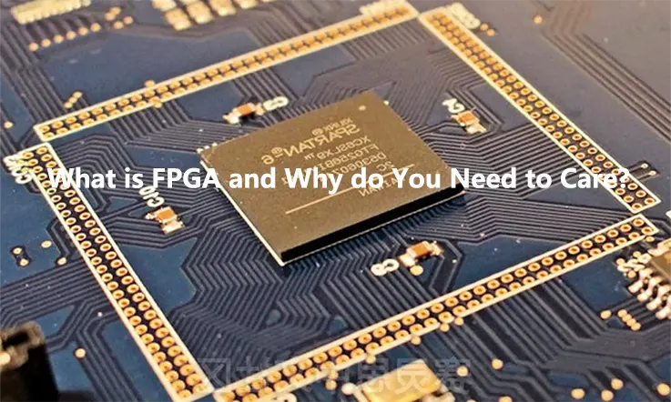
What Is FPGA ?
The Field Programmable Gate Array (FPGA) is a versatile type of integrated circuit that can be adapted to suit the unique needs of a specific application by utilizing user-programmable interconnects within its hardware blocks. An FPGA can facilitate the implementation of new functionalities throughout its lifespan due to its ability to reprogram its interconnects.
The design of FPGAs owes its origins to earlier devices like programmable read-only memories (PROMs) and programmable logic devices (PLDs). Though both PROMs and PLDs could be programmed either at the factory or in the field, their configurations were permanent and unalterable since they relied on fuse technology. However, FPGAs store their configuration information in reprogrammable mediums like static RAM (SRAM) or flash memory, offering greater flexibility.
Industry giants such as Intel, Lattice Semiconductor, Microchip Technology, and Microsemi are among the top manufacturers of FPGAs.
FPGA Architecture and Components
FPGA (Field Programmable Gate Array) consists of several architectural and component elements that enable users to program the circuit according to the required functionality. Here are some of the main architectural elements of an FPGA:
● Configurable Logic Blocks (CLBs): These are the basic building blocks of FPGAs, consisting of lookup tables (LUTs) for combinational logic, and flip-flops for sequential logic. In addition, some modern FPGAs have built-in math operations units, which come in handy for DSP applications.
● Programmable Interconnect: The interconnection gives the CLBs the tunnels through which data passes and by which signals from input and output pins are connected to the LUTs and flip-flops. In modern FPGAs, the interconnect uses a hierarchy of different types of routing wires, each with different speeds, directions, and lengths.
● Input/Output Blocks (IOBs): IOBs allow external signals to communicate with the internal CLBs and perform parallel or serial interfacing with other digital circuits/systems. The IOBs can handle a combination of single-ended, voltage-regulated, or differential signals and external clock signals.
● Embedded Memory Blocks: Some FPGAs have embedded memory blocks such as block RAM or FIFO buffers, available for designers to use either as a standalone memory or as an interconnection medium between modules.
● Digital Signaling Processing (DSP) Blocks: DSP blocks in the FPGA consist of multiple arithmetic circuits for performing complex math operations such as multiplication, division, and addition efficiently.
● Clock Management: FPGAs can offer various clock methods to ensure reliable and jitter-free clocking of internal modules or to connect to external synchronization requirements.
● Configuration Memory: The FPGA configuration information is stored in non-volatile memory such as Flash, ferroelectric, electrically erasable programmable read-only (EEPROM), or volatile Static RAM (SRAM), which will configure the FPGA at each start-up.
The interconnection between all these elements is programmable after manufacturing, allowing FPGA devices to provide a unique flexibility of configuration according to the intended application domain.
Advantages and Disadvantages of FPGA
Advantages of FPGA
●Flexibility: FPGA’s hardware configurability offers flexible and adaptable system designs which can be reprogrammed and reconfigured as needed.
●High Performance: FPGA’s parallel architecture can offer high performance, making it an excellent choice for applications requiring real-time processing and high-speed data processing.
●Lower Power Consumption: FPGA designs can offer lower power consumption compared to a software solution running on a CPU. This is because only the resources required to perform the task are used, and idle circuits are not powered up.
●Lower Cost: FPGA designs can offer a lower per-unit cost compared to ASICs designed for low volume applications, because the FPGA can be used for many different applications.
●Shorter Time to Market: FPGA provides shorter design cycles and reduces the time to market compared to a custom ASIC solution.
Disadvantages of FPGA
●Complexity: FPGA development can be challenging due to its complexity. Successful implementation requires extensive knowledge of digital logic design, hardware description languages, and FPGA technology.
●Higher Cost: High configuration costs of FPGAs as the initial investment is needed to buy the hardware and software design tools required for development.
●Limited Resources: FPGAs have limited resources compared to dedicated ASICs. This can result in limitations on the size and complexity of the designs that can be implemented.
●Limited Support: FPGAs requiring specialized knowledge of programming languages, and application programming interfaces (APIs) and hardware environments, that can limit technical support options.
Bitstream Security Concerns: Since bitstream is configurable data that controls the FPGA hardware functionality, it can be vulnerable to a malicious attack that alters the FPGA function.
FPGA Applications
The versatility of Field Programmable Gate Arrays (FPGAs) makes them a suitable option for numerous industries. As an industry leader, AMD provides comprehensive solutions for a diverse range of markets and applications. AMD’s offerings encompass FPGA hardware, advanced software, and configurable IP cores that are ready to be utilized.
AMD’s FPGA solutions are applicable to several markets and use cases, including:
●Wireless Communications: solutions for RF, base band, connectivity, transport, and networking for wireless devices, addressing standards such as WCDMA, HSDPA, and WiMAX amongst others.
●Wired Communications: Complete solutions for the Reprogrammable Networking Linecard Packet Processor, Framer/MAC, serial backplanes, and other components of the network.
●Aerospace & Defense: FPGAs that are resistant to radiation combined with the intellectual property necessary for image processing, waveform synthesis, and partial reconfiguration of SDRs.
●ASIC Prototyping: The use of field-programmable gate arrays (FPGAs) for ASIC prototyping enables rapid and precise modeling of SoC systems as well as verification of embedded software.
●Video & Image Processing: For a variety of video and image applications, AMD FPGAs and tailored design platforms allow better levels of flexibility, quicker time-to-market, and reduced total non-recurring engineering expenditures (NRE).
● Automotive: Providing automotive silicon and intellectual property solutions for gateway and driving assistance systems, as well as comfort, convenience, and in-vehicle infotainment systems.
● Security: Access control, surveillance, and other safety and security systems are just some of the areas in which AMD has developed solutions to satisfy the ever-changing requirements.
● Broadcast & Pro AV:With Broadcast Focused Design Platforms and solutions for high-end professional broadcast systems, you can adapt to changing requirements more quickly and lengthen the product’s life cycle.
● Medical:The Virtex FPGA family and the SpartanTM FPGA family can both be used to meet a variety of processing, display, and input/output interface requirements for applications such as diagnosis, monitoring, and therapy.
● Consumer Electronics:Converged handsets, digital flat panel displays, information appliances, home networking, and household set top boxes are all examples of next-generation consumer applications that can take advantage of cost-effective solutions.
● Industrial: Applications ranging from industrial imaging and surveillance to industrial automation and medical imaging equipment can all benefit from the increased flexibility, accelerated time-to-market, and decreased overall non-recurring engineering costs (NRE) made possible by AMD FPGAs and ISM-specific targeted design platforms.
● Data Center: Developed specifically for servers, networking, and storage applications that require high bandwidth and low latency in order to deliver a higher level of value to cloud deployments.
● HighPerformance Computing and Data Storage: Storage area networks (SAN), network-attached storage (NAS), servers, and storage appliances can all benefit from these solutions.
Programming Process an FPGA Design
Programming an FPGA involves describing the desired hardware functionality in a hardware description language (HDL), compiling the HDL code into a configuration bitstream, and then loading the bitstream into the FPGA. The general steps in programming an FPGA are:
●Design Entry: Write the hardware functionality in a HDL such as VHDL or Verilog, which describe the FPGA’s hardware behavior.
●Synthesis: The HDL code is translated into an optimized netlist, where the synthesis tool configures the FPGA with the desired functionality. This step creates a structural representation of the logic.
●Mapping:Mapping the synthesized netlist onto the FPGA architecture specified in the design.
●Placement: Placement of synthesized logic blocks on the FPGA floorplan that maximizes performance and timing.
●Routing: Creation and optimization of the interconnects, to connect the placed blocks together and to the input/output pins.
●Timing Analysis: Timing Verification and analysis to ensure the design timing requirements are correct.
●Bitstream Generation: Generation of a binary data file containing instructions for configuring the FPGA, known as “bitstream.”
●Configuration:Download the bitstream onto an FPGA device to configure the FPGA according to the specified design.
●Verification:Verify that the FPGA implementation matches the expected behavior.
Hardware description languages, such as VHDL and Verilog, offer a highly structured way of describing the behavior of digital systems and are used to create complex systems spanning a range of industries. FPGAs can also be programmed using high-level programming languages, such as C and C++, with the help of hardware design libraries such as High-Level Synthesis (HLS).
How FPGAs Work ?
FPGAs or Field Programmable Gate Arrays are integrated circuits that can be programmed or configured to perform specific tasks after manufacturing. Here is a high-level description of how FPGAs work:
● FPGA design: The first step is to create a design using a hardware description language (HDL) such as Verilog or VHDL. The design is usually created using a computer-aided design (CAD) tool.
● Synthesis: Next, the design is synthesized to produce a netlist, which is a high-level representation of the circuit.
● Place and Route: The place and route process takes the netlist and maps it onto the physical resources of the FPGA, including logic cells, routing switches, and input/output pins.
● Configuration: Once the netlist has been placed and routed, the FPGA must be configured with the appropriate settings using configuration memory such as flash memory or SRAM. This step sets the electrical path, logical connection and creates the interconnects between the devices.
● Operation: After configuration, the FPGA performs the programmed function and can be updated with new functions by reprogramming the configuration memory.
FPGAs can be reprogrammed repeatedly and can execute parallel operations as well as displaying lower power consumption in comparison to alternatives.
Why You Use a Field Programmable Gate Array ?
With FPGAs, you can tune your chip such that it can handle a high workload. So, when working with these chips, you may acquire the best possible outcomes. In addition to this, FPGA enables you to make later modifications at the chip level to produce the outputs that you want. Because of this level of adaptability, you are able to make significant modifications. For instance, you can adjust the power and memory use of your machine by making use of FPGA in order to save up on resource utilization. That could end up being a savior for your device in the end.
When it comes to the prototype of ASICs (Application-Specific Integrated Circuits) or Processors, FPGAs can prove to be quite helpful. This is due to the fact that you are able to re-program an FPGA until you obtain a final, bug-free Processor or ASIC that you are able to mass produce.
Comparison of FPGAs with Other Types of Programmable Logic Devices
FPGAs are one type of programmable logic device, and there are several other types available as well. Here is a comparison of FPGAs with other types of programmable logic devices:
● CPLDs (Complex Programmable Logic Devices): CPLDs are smaller and slower than FPGAs and generally used for simpler designs. They usually have a fixed architecture with a limited number of programmable elements.
● PALs (Programmable Array Logic): PALs are an early type of programmable logic device, and they have a fixed number of inputs and outputs. The logical functions are implemented using a programmable AND array followed by a fixed OR array.
● GALs (Generic Array Logic): GALs are similar to PALs, but they have additional programmable features such as flip-flops and control circuits, thus being more flexible than PALs.
● ASICs (Application-Specific Integrated Circuits): ASICs are custom-designed integrated circuits that are optimized for a specific application. They typically have higher performance and lower power consumption than FPGAs, but are more expensive and have longer design time.
Compared to CPLDs, PALs, and GALs, FPGAs are larger, faster, and more flexible. They offer a large number of programmable logic elements, optimized routing, and other features that allow designs to be implemented in a more optimized way. When compared with ASICs, FPGAs are more flexible at design time, provided design modifications are quicker and can be tested easily.
ASIC Vs. FPGA
Choosing between ASICs and FPGAs requires a thorough evaluation of each technology’s unique benefits. Numerous comparisons between the two types of technologies are available online. Historically, FPGAs were more suitable for designs with lower levels of complexity, speed, and overall volumes. However, modern FPGAs are capable of achieving performances of up to 500 MHz and beyond while boasting significant improvements in logic density, embedded processors, clocking, high-speed serial, and DSP blocks at increasingly affordable prices. As a result, FPGAs have become an attractive option for a broad range of designs.
Compared to microprocessors like ASICs, FPGA designs offer three significant advantages, particularly for prototypes or limited production runs. These advantages include:
●Performance of Flexibility: FPGAs are not often utilized in heavily parallelized processes due to the inability to match the performance of CPUs. Applications such as large image processing and digital signal processing require numerous cores and out-of-order instructions that current microprocessors execute better.
Furthermore, FPGA designs can incorporate several hard or soft microprocessors working together in a single chip. This integration eliminates the need to physically connect two separate devices, thus reducing the required space for the design.
FPGA design cycles require less manual intervention and are easier to manage due to their simpler nature. Routing, positioning, and timing are often handled automatically by the software to ensure compliance with specified criteria.
●Reusability: The versatility of FPGAs as reprogrammable and reusable devices makes them highly adaptable for rapid prototyping, with minimal costs associated with design mistakes or modifications.
FPGAs have a distinct advantage over ASICs due to their reconfigurable capability. Once the system has been established, FPGAs offer the ability to reconfigure repeatedly, enabling further modifications, optimization, and customization that ASICs cannot achieve. This capability is despite an intricate and detailed IP core design for a specific application. The true value of FPGAs lies in their reprogrammability, which provides PCB design engineers with increased flexibility for future design iterations and modifications.
●Quick Acquittance: FPGAs offer a shorter time-to-market advantage because they are not pre-designed for specific activities. After purchasing an FPGA, it can be configured to fit the required design specifications. This flexibility is valuable for PCB design engineers, as they can potentially reduce development time and rapidly prototype with FPGAs, leading to a quicker time-to-market.
Programming Languages and Tools for FPGAs
There are several programming languages and tools available for designing FPGAs. Here are some commonly used ones:
● Hardware Description Languages (HDLs): HDLs like Verilog and VHDL are used to create the digital circuit designs that implement the required functions. HDL-based designs are transformed by logic synthesis tools into a netlist of primitive digital logic elements (gates, LUTs, flip-flops, etc.) and connected by logic synthesis tools into a full digital circuit design.
● High-level synthesis (HLS) tools: These tools allow designers to write code in a high-level language such as C/C++, Python or even OpenCL, which is then automatically converted into a hardware description language or a netlist-based design using various optimization criteria. This can significantly reduce design time and provide higher-level abstraction.
● FPGA Development Platforms: FPGA vendors offer development platforms, which include software for design compilation, simulation, synthesis, and debugging. They provide a comprehensive workbench for test and builds utilizing integrated development environments (IDEs).
IP Cores: Intellectual property cores are pre-built blocks of design (i.e. memory, processors, communication interfaces, etc) provided by FPGA vendors to accelerate complex designs or applications development, frequently tailored for specific uses.
● High-Level Design Tools: Commercial high-level tools such as MATLAB, Simulink, or LabVIEW provide integration with FPGA design flows to create and validate designs faster and more efficiently.
The selection of tools and languages may depend on a variety of factors such as the designer’s experience, the complexity of the design, and the specific requirements of the project.
Why an FPGA when a Microcontroller Would Do ?
Choosing between an FPGA and a microcontroller depends on whether the design requires software or hardware functions.
● A microcontroller operates by executing instructions sequentially, which imposes inherent limitations. The intended functionality must align with the available instructions, and performing multiple processing jobs at the same time is generally not feasible. Although instructions are highly flexible and can be executed at high frequencies, software-based digital design still has drawbacks.
● A hardware-based approach is an alternative. Ideally, each new design could be created with a digital IC tailored to the required system functionality. There would be no software development, no instruction set limitations, and no processing delays. The result would be a single IC with input and output pins and digital circuitry designed precisely for the required operations.
● Developing an ASIC for each board is impractical, but FPGAs offer a more practical solution that approximates the process. FPGAs provide the flexibility of reprogrammability to allow digital circuits to be modified to meet specific design requirements. This approach combines the best of both worlds by offering hardware implementation with the flexibility of software-like modifications.
Importance of FPGA
Field-programmable gate arrays (FPGA) are important due to the following reasons:
●Flexibility and Programmability: FPGA offers high flexibility and reprogrammability, which advantages the design of complex digital systems. It is possible to reconfigure the FPGA multiple times, which makes it easy to modify, test, and redesign the system until it satisfactorily meets the requirements. The FPGA’s highly flexible architecture provides an ideal platform for prototyping digital circuits and systems.
●High Performance and Low Power Consumption: FPGAs provide high performance and low power consumption, which makes them suitable for many applications such as, digital signal processing, image, and video processing, artificial intelligence, etc. FPGA provide parallel processing, which improves the computational performance by performing multiple operations at the same time. FPGA design can be optimized for the specific task, reducing the power consumption compared to the general-purpose CPUs.
●Rapid Prototyping: FPGA introduces a faster design and prototyping cycle, and it removes the barriers that traditional ASIC design may possess regarding the time, costs, and effort invested in the design and fabrication of custom chips. FPGA speeds up the prototyping process by delivering an environment that enables designers to implement, validate and upgrade their circuits with no need to have a physical board.
●Hardware Emulation: FPGA is capable of emulating other electronic hardware devices or circuits for testing and debugging purposes eliminating the need for the physical device. It simplifies the test setup, saves research time and further cost, and makes it practical to run tests on complex systems.
Therefore, the FPGA is essential in modern electronics and is increasingly important with the growth of industries such as robotics, IoT, artificial intelligence, and wireless communications. Its customizable and reconfigurable nature makes it suitable for use in research, prototyping, and commercial product development.
Get to More Understand About FPGAs
● The high tooling and pre-production expenses required for custom ASICs make them unsuitable for low to medium scale high-tech products, but they are a great solution for high-volume applications. Instead, for these products, field-programmable gate arrays (FPGAs) are frequently used. These large-scale integrated chips consist of a collection of logic gates, primarily NAND gates, which can be programmed by the manufacturer to carry out a predetermined set of logical operations, meeting specialized requirements.
● PROMs and PLDs were developed in the 1970s and have been succeeded by the current generation of FPGAs. The most notable difference is that FPGAs can be reprogrammed in-circuit by manufacturers, simplifying device management in contrast to pre-programming devices before leaving the factory.
● Modern FPGAs now incorporate analog functionalities, allowing them to integrate more closely with digital functions. These integrations include features such as programmable slew rates, analog-to-digital converters, and differential comparators. This blurring of the lines between FPGAs and Field-Programmable Analog Arrays (FPAAs), which are analog devices, has resulted in the modern FPGAs being capable of analog and digital functions.
FPGA Trends and Future Developments
The trends and future developments in the field of FPGAs include:
● FPGA vs. ASIC: A continued trend is the ongoing competition between FPGAs and ASICs (Application-Specific Integrated Circuits), as both technologies are used for hardware acceleration and optimization. FPGAs offer more flexibility and shorter design cycles, while ASICs offer higher performance and lower power consumption.
● FPGA in the Cloud: Another trend is the use of FPGAs in cloud computing. Cloud providers such as Amazon Web Services, Microsoft Azure, and Alibaba Cloud offer FPGA instances as a service, enabling customers to use FPGAs for various applications without the need for upfront investment in hardware.
● FPGA for AI and Machine Learning: FPGAs offer high parallelism and flexibility, making them well suited for accelerating computationally intensive applications like AI and machine learning. FPGAs can perform tasks such as image and speech recognition, natural language processing, and recommendation systems with high performance and low power.
● Heterogeneous Computing: FPGAs are expected to be more widely used alongside other processing elements such as CPUs and GPUs in heterogeneous computing systems. This allows for the optimization of performance while minimizing energy consumption.
● High-Speed Connectivity: With the growing demand for high-speed connectivity, FPGAs are being used to develop solutions for 5G communications, data centers, and other high-performance networking applications.
● Security: FPGAs have been gaining attention as a potential solution for hardware security. By embedding security mechanisms within the FPGA fabric, it is possible to create secure systems that are resistant to cyber-attacks.
In a word, the demand for FPGAs is expected to continue to grow, as they provide a flexible and powerful tool for hardware acceleration and optimization in a wide range of applications.
Conclusion
Field-Programmable Gate Arrays (FPGAs) are both fascinating and highly effective devices, offering several benefits beyond reducing resource consumption. They can help save significant costs while keeping up with industry developments. Therefore, incorporating FPGAs into a project is a wise decision.
Understanding the fundamental aspects of FPGAs and their advantages over processor-based systems can be beneficial. Designers familiar with microcontrollers, ASICs, and mathematical calculations may initially find modern FPGAs intimidating due to their complexity and high performance. However, enhancing performance and versatility in certain applications may justify the additional design effort required.
In a word, FPGAs provide significant benefits to PCB design engineers. Understanding their features and capabilities can allow designers to make well-informed decisions when selecting digital system components, ultimately leading to developing high-performance and cost-effective electronics solutions.
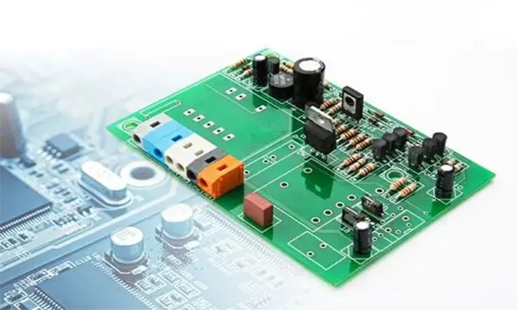
The demand for carrier printed circuit boards (PCBs) is increasing in tandem with the growing complexity and miniaturization of electronic equipment and systems, as well as the need for improved signal integrity, lower power consumption, and higher data rates. Carrier PCBs serve as a stable and reliable platform for configuring and interconnecting multiple electronic components, including microprocessors, memory chips, sensors, and power devices.
The development of carrier PCBs is being driven by several key trends. Firstly, there is increasing adoption of advanced materials and fabrication methods such as HDI (high-density interconnect) and microvia technology, which allow for denser component placements and shorter signal paths. Secondly, the integration of passive and active components directly onto the PCB substrate is gaining prominence, enabling manufacturers to design more compact and efficient electronic systems.
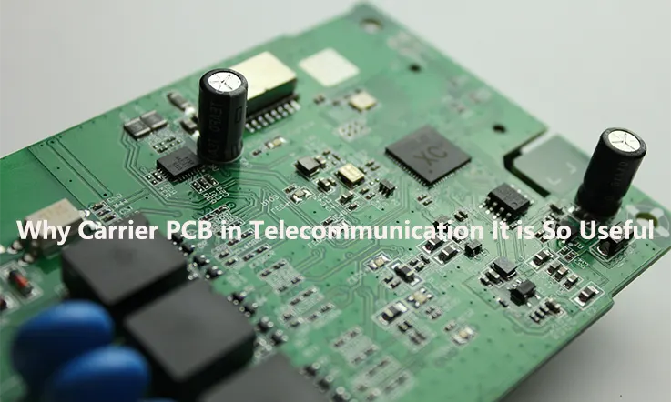
In addition, the importance of Carrier PCB in telecommunication lies in its ability to provide a reliable platform for transmitting and receiving data at high speeds, while also managing power consumption and reducing interference. With the increasing demand for faster and more efficient communication systems, Carrier PCB has become an indispensable part of modern telecommunication technology.
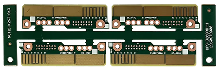
What Is Carrier PCB ?
A Carrier PCB, also known as a Printed Circuit Board, is utilized within the electronics industry to provide a solid platform with the necessary connectivity required to successfully host and integrate a diverse range of electronic components, modules, or circuit boards. This type of PCB simplifies the process of testing, prototyping, and manufacturing by offering a standard interface between the carrying PCB and the components it hosts.
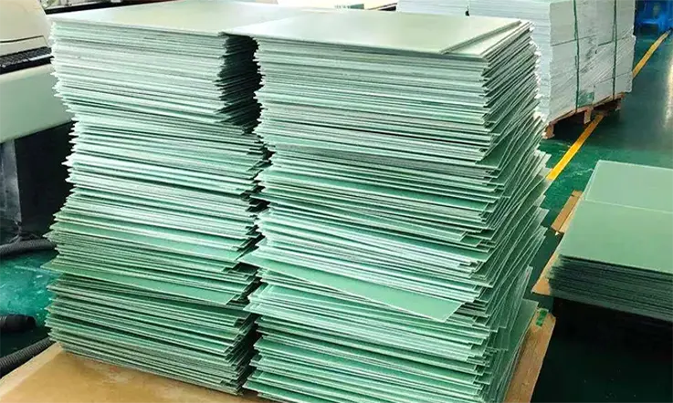
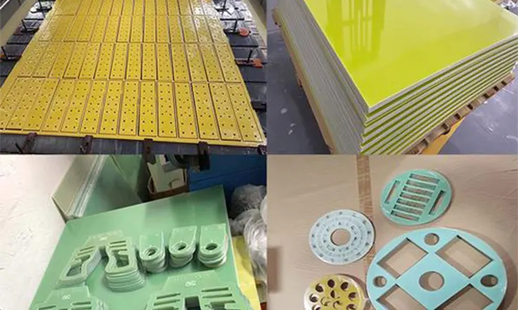
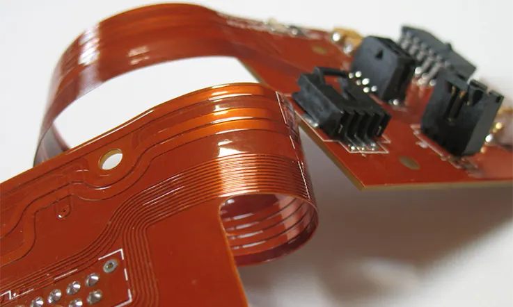
Carrier PCBs can significantly improve the system’s overall reliability and maintainability by providing standardized connectivity between electronic components without requiring extensive customization or modification. Furthermore, these customized boards can be fabricated from a range of materials, such as polyimide, FR-4, or flexible materials, depending on their intended application and specific design requirements.
Advantages and Applications of Carrier PCB in Telecommunication
Carrier PCB is widely used in telecommunication systems due to its numerous advantages and applications, some of which include:
●High Speed Transmission: Carrier PCBs are designed with high-quality materials and advanced features to enable fast and reliable data transmission with reduced signal loss and attenuation.
●Enhanced Signal Integrity: Carrier PCBs are designed to reduce noise and electromagnetic interference (EMI), which helps enhance signal integrity and minimize errors in data transmission.
●Power Management: Carrier PCBs have advanced power management features that help manage power consumption and distribution in telecommunication systems, ensuring that power is utilized efficiently and effectively.
●Noise Reduction: Carrier PCBs are designed to reduce noise and interference from other circuitry and external sources, ensuring that telecommunication systems operate with minimal disruption.
●Versatility: Carrier PCBs can be used in a wide range of telecommunication applications, including cellular networks, internet routers, satellite communication systems, and more.
● Cost-Effective: Carrier PCBs offer a cost-effective solution for telecommunication systems design and manufacturing, providing high-quality performance at a relatively low cost.
How Carrier PCB Is Designed ?
Carrier PCB (Printed Circuit Board) design involves several crucial steps, including material selection, layer stackup configuration, trace routing, and component placement. Here’s a brief overview of each step:
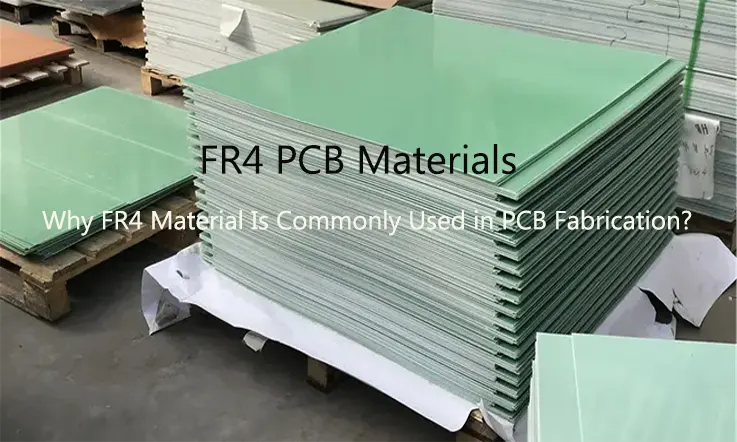
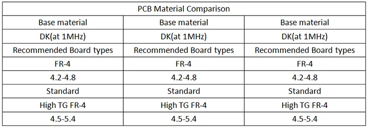
● Material Selection: The choice of materials for Carrier PCB design is critical and depends on factors such as the frequency of operation, thermal management requirements, and cost. Materials commonly used for Carrier PCBs include FR-4, Rogers, and Isola.
● Layer Stackup Configuration: The layer stackup configuration involves determining the number and placement of copper layers in the PCB. The stackup configuration is crucial as it affects signal integrity and the routing of traces.
●Trace Routing: Trace routing involves the routing of copper traces on the PCB to connect components and carry signals. This step requires careful consideration of factors such as trace length, impedance control, and noise reduction.
● Component Placement: Component placement involves the positioning of electronic components on the PCB. Component placement affects signal integrity, thermal management, and the routing of traces on the board.
Factors to Consider for Optimal Carrier PCB Design
For optimal Carrier PCB (Printed Circuit Board) design in telecommunication systems, various factors need to be considered, including:
Signal Loss and Attenuation: Signal loss and attenuation occur when a signal travel along a trace, and its amplitude reduces due to various factors like transmission line impedance, dielectric constant, frequency, and trace routing. Good impedance control and keeping trace routing shorter can help reduce signal loss and attenuation.
Crosstalk and Electromagnetic Interference:Crosstalk and Electromagnetic Interference (EMI) are major sources of signal interference in telecommunication systems. To minimize these effects, Carrier PCB design should incorporate proper ground planes, shielding techniques, and careful trace routing.
Thermal Management: Telecommunication systems often generate significant heat due to high-speed processing and power consumption. Carrier PCB design should incorporate proper heat sinking techniques and the use of materials with high thermal conductivity to manage heat dissipation.
Board Size and Shape: The size and shape of the PCB can affect signal integrity, and board layout can substantially impact trace routing. Careful consideration should be given to board design to optimize board size and shape for efficient signal transmission.
How Does Carrier PCB Technology ?
PCB (Printed Circuit Board) technology is used in a wide range of electronic devices, including carrier PCBs. Carrier PCB technology refers to the design and manufacture of circuit boards that are used to carry or transport other electronic components, such as microprocessors, memory chips, or other integrated circuits.
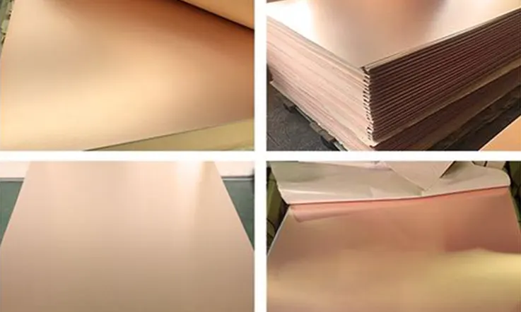
A carrier PCB is essentially a support structure that provides a physical and electrical connection between the electronic components that are mounted on it. The carrier PCB typically has a number of layers, with each layer containing a network of conductive pathways that are used to connect the various components. These conductive pathways are typically made of copper, and they are etched onto the surface of the PCB using a process known as photolithography.
The process of designing and manufacturing a carrier PCB typically involves the following steps:
PCB Design:The first step in creating a carrier PCB is to design the layout of the circuit board. This involves deciding which components will be mounted on the board, and how they will be connected.
PCB Fabrication: Once the design is complete, the next step is to fabricate the PCB. This involves using a process known as photolithography to create the conductive pathways on the surface of the board.
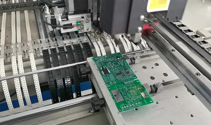
PCB Assembly:Once the PCB has been fabricated, the next step is to assemble the electronic components onto the board. This involves placing the components onto the board and soldering them into place.
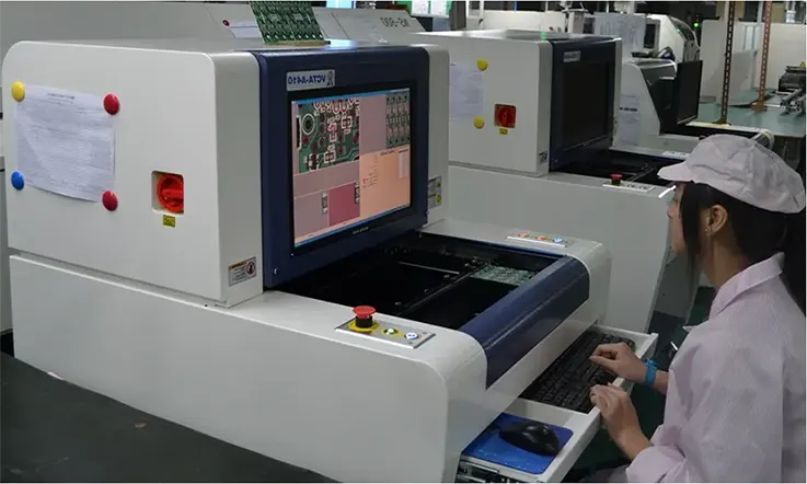
Printed Circuit Boards Testing: Finally, the carrier PCB is tested to ensure that all of the components are properly connected and functioning as intended.
Carrier PCB technology is used in a wide range of applications, including in telecommunications equipment, industrial machinery, and consumer electronics. It provides a cost-effective and reliable way to connect and transport electronic components, and it is an essential component in many electronic devices.
Real-World Applications of Carrier PCB in Telecommunication
There are various real-world applications of Carrier PCB (Printed Circuit Board) in telecommunication systems. Here are some case studies:
● Cellular Networks: Carrier PCBs are extensively used in cellular network base stations, enabling high-speed data transmission with minimal signal loss and EMI. Carrier PCBs also allow for power distribution management, which helps maximize the efficiency of cellular network systems.
●Internet Routers: Carrier PCBs play a significant role in internet routers and switches, enabling efficient and reliable data transmission across networks. For high-speed data routing, advanced Carrier PCB design techniques such as Backdrilling and Blind Via technology are used.
●Satellite Communication: Carrier PCBs are used in satellite communication systems, where high-speed and reliable data transmission is essential. The use of Carrier PCB allows for better impedance control, which helps prevent signal loss due to reflection.
● Military Communication Systems: Carrier PCBs are used in military communication systems such as satellite communication, ground systems, surveillance, and radar systems. The use of Carrier PCB allows for efficient power distribution, precise signal routing, and high-speed communication.
● Industrial Automation and Control Systems: Carrier PCBs are used in Industrial Automation and Control Systems (IACS) to provide stable, high-speed communication, and efficient power distribution. IACS often requires a higher degree of resistance to harsh environmental conditions, and Carrier PCBs with high-temperature capabilities and environmental resistance are used to address this.
Carrier PCB Networks in Phones: Their Purpose
Mobile devices rely on being connected to a network comprised of base stations and interconnections for radio equipment that enable data transmission. These essential components are owned by the carrier PCB network, including the radio spectrum utilized by serviced phones.
Telecommunications firms responsible for maintaining the network infrastructure and radio airwaves facilitate both direct service to end-users and the provision of wireless carrier services to other companies. Wireless carriers may also use other names, such as mobile phone providers or mobile service providers.
Certain mobile phone service providers may only resell the services of larger carriers and lack the necessary infrastructure. Mobile Virtual Network Operators are examples of such companies as they use the networks of established operators to provide services to their customers.
The importance of carrier network resilience is underscored by an ever-increasing demand for cellular data services. 5G-NR, the newest performance standard for cellular technology, offers faster speeds than the current 4G LTE network to wireless broadband routers and mobile devices.
Accommodating this expansion requires additional wireless spectrum and faster backbone connectivity to wireless stations. Otherwise, slow connections and network congestion will occur if capacity fails to keep up with growing demand.
Carrier PCB’s Crucial Role in the Field of Telecommunications
The internet heavily relies on data carrier circuit boards that underpin the transmission of vast amounts of data. Data often passes through numerous carrier networks before reaching the end user. Some networks may choose to waive fees for specific partners, while others may charge fees to transmit data to other networks.
● In the telecommunications industry, carrier boards play a critical role as components incorporated into the carrier system to facilitate the transmission of information, such as voice signals and video signals, through modulation of one or more high-frequency carrier signals above the primary voice frequency and data rate.
● Through multiplexing various carrier signals, a single carrier board is capable of simultaneously transmitting numerous communication channels through a shared medium. Among the different multiplexing techniques, frequency-division multiplexing and time-division multiplexing are the most common, with frequency-division multiplexing being used in cable television networks to transmit various television shows at different frequencies.
● Time-division multiplexing is utilized in public switched telephone networks to route a significant number of calls through a single trunk line. For long-distance phone conversations, frequency-division multiplexing is a viable option, allowing multiple channels to be transmitted via satellite connections. Individual channels can be demultiplexed at a particular receiving node.
Challenges and Future Directions for Carrier PCB in Telecommunication
While the use of Carrier PCB (Printed Circuit Board) has revolutionized the telecommunication industry, various challenges and future directions need to be considered, including:
High-Speed Performance: As telecommunication systems evolve to meet the ever-increasing demand for faster speed, Carrier PCB design must be optimized for high-speed performance. This requires specialized design techniques to minimize signal loss and noise while maintaining signal integrity.
●5G Technology: The advent of 5G technology presents unique demands for Carrier PCB design, such as higher frequency operation, wider bandwidth, and increasing power consumption. As such, future Carrier PCB designs must address these challenges.
●Power Consumption: Energy efficiency is an important consideration in Carrier PCB design, as telecommunication systems consume a lot of power. Future designs must focus on minimizing power consumption and optimizing power management strategies.
●Miniaturization: The trend towards smaller and more portable telecommunication devices presents challenges for Carrier PCB design, such as the need for smaller traces, denser component packing and more complex routing.
● Cost: Despite its advantages, Carrier PCB production costs can be high, with material costs and production being a significant expense. Future Carrier PCB designs must address cost issues and seek to provide cost-effective solutions.
Therefore, addressing these challenges and focusing on future directions is essential for Carrier PCB innovation and expanding its role in telecommunication systems.
Conclusion
The carrier PCB plays a crucial role in transmitting data either via electromagnetic waves or by enabling frequency division multiplexing. Its capacity for both functions makes it an integral component in many electronic systems.
As a renowned PCB manufacturing and assembly factory in China, Janistech offers a broad range of custom PCB manufacturing services, including Medical Rigid-flex PCB, HDI PCB, Metal Core PCB, Ceramic PCB, and Carrier PCB, among others. To access our services for your upcoming PCB project, please contact us via email at [email protected]. We will respond promptly and offer expert assistance to ensure your satisfaction.
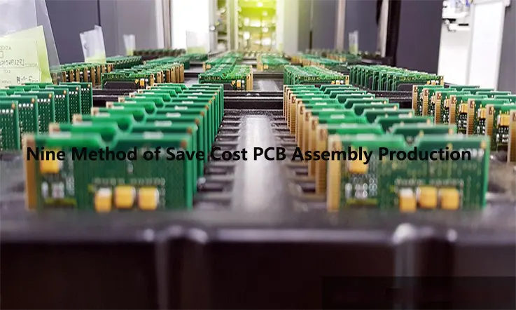
In today’s highly competitive industrial landscape, engineers are constantly seeking out innovative means of reducing the cost of their products without compromising on quality. Printed Circuit Boards (PCBs) are a crucial component of electronic and electrical engineering hardware, and their cost has a substantial impact on the price of the final product. Therefore, selecting a cost-effective PCB assembler and manufacturer that offers superior quality at reasonable prices is vital.
However, it has come to our attention that several providers offering cost-effective prototype PCB assemblies compromise on quality, resulting in product failures and noncompliance. To strike a balance between the cost and quality of PCB assembly, it is imperative that customers scrutinize the portfolio, services, and terms & conditions offered by each PCB assembler. Customers must also bear in mind their financial constraints while selecting an assembler and optimize their circuit design or PCB layout during the design phase.
To reduce the cost of PCB assembly effectively, customers must be cognizant of the challenges of cost optimization and quality control. By following these guidelines and collaborating with a reliable PCB assembler and manufacturer, customers can cut costs while ensuring that the quality of their products meets or exceeds their expectations.
What Factors Contribute to the High Cost of PCB Assembly ?
The cost of PCB design and production is influenced by various factors such as the intricacy of the design, the types of parts used, and the overall efficiency of the project. Additionally, the complexity and characteristics of the circuit are crucial elements that impact the total cost of PCB construction. Furthermore, the quality of PCB design can play a vital role in the final price.
The use of leadless components, coupled with precise pitching, adds to the overall expense of the PCB assembly. This is primarily due to the need for distinct testing procedures and a unique assembly process. The cost of essential components is also a significant factor contributing to the high cost of PCB assembly. The fabrication and assembly of printed circuit boards (PCBs) are reliant on sophisticated technology that caters to the demands of various industries. Consequently, the cost of PCB assembly is directly dependent on the firms, products, and assembly strategies involved.
Furthermore, there are three critical aspects related to the cost of the PCB that must be considered during PCB assembly:
● High-cost raw materials can lead to increased PCB production expenses.
● Unforeseen abnormalities that arise during production necessitate retesting at every stage of the assembly process.
● The assembling process has a significant impact on both the performance and cost of the resulting PCB.
How Can I Have Professionals Reduce PCB Assembly Cost ?
The cost of printed circuit board (PCB) assembly is frequently influenced by multiple factors, including the quantity and type of components and the intricacies of the assembly process. Different PCB assembly providers may use distinct pricing methods, causing pricing variations to occur.
Despite having no control over the assembly process, specific design strategies may be leveraged to reduce the overall cost of PCB assembly. By implementing such tactics, you can achieve your cost-effective goals and successfully reduce PCB assembly expenditures.
● Putting Surface-mount Parts on Just One Side: The cost of manufacturing a printed circuit board (PCB) with surface-mounted devices (SMD) on both sides is typically higher than that of a PCB assembly with SMDs on one side. This is because the process requires only a single pick and place setup iteration, resulting in significant cost savings for the stencil.
● Proper Designator Labeling: Designators are an essential component of PCB layout as they aid in component identification on the printed circuit board. They should be positioned in proximity to the corresponding components and be easily recognizable. The inclusion of designators simplifies the setup process for PCB assemblers and reduces the likelihood of issues arising during hand placement.
● Panelize The PCB: For mass production of circuit boards (PCBs), it is advisable to produce them in panels to reduce costs and streamline the assembly process. Manufacturing multiple iterations of the same printed circuit board (PCB) in a single panel reduces the number of PCB assembly runs.
During the pick and place process, it is crucial to ensure that the PCB panels contain sufficient fiducial markers to maintain accurate orientation. Fiducial markers are visual cues that aid in effective pick and place machine operation, and their inclusion in the PCB panel is highly recommended for maintaining precision in automated assembly processes.
● Give A Full BOM List: Generating a Bill of Materials (BOM) is a critical step during PCB layout development. This step is often considered less crucial than Gerber generation; however, it holds more significance. BOM assists the assembler by enabling them to place components on the appropriate footprint. It also aids in procurement planning and budgeting by allowing optimization of quantity and usage.
Generated by a designer, BOM files are essential for PCB assemblers to acquire the correct components and materials and initiate PCB assembly. Incomplete BOM files may lead to unnecessary delays and the procurement of inappropriate components, resulting in wasted time and expenses. The BOM should include the name of the supplier and manufacturer, part number, quantity, reference designator, and details regarding the parts and package footprint.
Several PCB assemblers offer their own BOM generation forms. When completed by the designer and provided to the assembler, it leads to a faster assembly process. Moreover, designers should consider providing alternative component replacement options, including replacement part numbers on the BOM. While constructing a circuit, a specific IC package may no longer be available on the market, making finding an alternative replacement a difficult task. Providing alternatives saves the assembler’s time searching for parts that are no longer accessible, reducing delays in production.
● Adjust Order Quantity: Order volume plays a significant role in reducing the overall costs of a PCBA. In general, the cost per unit decreases as larger quantities are ordered, whereas smaller quantities result in higher per-unit costs. This holds true for both bare and populated PCBs, as well as electronic components such as ICs, resistors, and capacitors. Therefore, there exists an inverse relationship between cost and quantity or order volume.
It is crucial to ensure that the PCB assembler can deliver your required specifications while also considering your order quantity requirements. When developing prototypes in quantities of 1 to 5 pieces, the cost per piece unavoidably tends to be higher compared to bulk or higher-volume orders.
● SMT Assembly Price is Cheaper Than Through-hole Assembly: Most modern electronic production facilities utilize Automated Surface Mount Technology (SMT), as it is a cheaper production method in terms of labor cost for custom PCB board production.
While hand placement is still used for Through-Hole Technology (THT), which has been in use since the inception of the industry, it is now mostly supplanted by SMT technology. Although certain connections that are subject to heavy stress, such as power connections, may still require THT, for the most part, SMT has taken over.
It is essential to minimize the number of through-hole operations in the manufacturing process as it contributes to higher costs for custom PCB design. In conclusion, the use of SMT has become the preferred technology, owing to its cost-effectiveness in modern PCB assembly manufacturing.
● Design Complexity: In order to minimize costs during PCB assembly, it is advisable to keep the layout complexity to a minimum. Additional work for the manufacturer, required to realize elaborate designs, can increase costs. One example is ensuring that all components are located on the same side of the circuit board, avoiding the need for surface mounting twice.
However, complexity may be unavoidable in certain instances. For instance, further scrutiny may be required for the inspection of specific design elements like ball grid arrays (BGAs). Similarly, some elements like conformal coating might necessitate an additional assembly phase, despite being necessary. This coating protects mining equipment and medical instruments from dust and vibration but is unfortunately often expensive.
● Lead Time: Expedited PCB orders entail a higher cost, akin to that of the United States Postal Service. If an ECM or bare PCB boards is given a shorter turnaround time to complete the project, it will charge a higher rate. In such cases, the producer may need to source resources from within the United States instead of other countries, thereby incurring higher costs. Unfortunately, manufacturing costs in the United States are higher than those in China, as widely acknowledged.
Moreover, the choice of components influences the lead time. By specifying readily available components that are already in stock, it becomes easier for the contractor to expedite the project completion process.
● Outsourcing Your PCB Services: Many business owners mistakenly believe that assuming as many responsibilities as possible themselves can save costs. However, this DIY approach often falls short in the long run. Despite potentially spending less initially, production delays, design flaws, and other factors can increase overall costs. The equipment and materials used in-house may not match the quality that outsourcing to a professional PCB manufacturer can provide. Ultimately, partnering with a PCB manufacturer can offer access to superior tools, high-quality products, and overall cost reductions.
While managing costs is a valid concern, it should not impede PCB initiatives. Contact us today to learn more about our services.
Importance of Cost-saving in PCB Assembly Production
Cost-saving in PCB assembly production is important because it directly impacts the profitability of the final product. By reducing the cost of PCB assembly production, a company can increase its profit margin, maintain competitiveness in the market, and invest resources into research and development of new products. Additionally, cost-saving measures can improve overall manufacturing efficiency, reduce defects and production errors, and enhance the quality of the end product. Therefore, an emphasis on cost-saving in PCB assembly production is essential for long-term business success.
Conclusion
Maintaining a long-term partnership with a single PCB assembler or manufacturer is advantageous for your company. Engaging in trial and error with products from different manufacturers cannot produce consistent results. It is therefore important to foster strong mutual cooperation and trust with your PCB assembler to achieve greater goals and generate more business. This, in turn, may result in lower pricing for your orders.
It is crucial to keep in mind that the cost of PCBA for an electrical device project is just a small portion of the overall expense. While prices may vary based on the supplier and location, they are not the primary factor driving up costs.
In modern times, electronic manufacturing companies are designing increasingly complex printed circuits with multiple layers, causing a surge in the importance of PCB stackup design. It is common knowledge that a well-designed stackup is crucial for reducing radiation from PCB loops and associated connections. Conversely, a poorly designed stackup can significantly increase radiation levels, posing potential safety hazards.
The growing demand for smaller electrical goods compels companies to use PCBs with multiple layers and a three-dimensional design approach, leading to new challenges in design tactics like SMD packaging and layer stackup. As printed circuits become ever more sophisticated, with a high number of layers, the stackup or stack of PCBs has gained increasing importance in design considerations. Compared to earlier times when PCB designs were rudimentary and only served as a platform for connecting electronic components, there was minimal need for multi-layer stacking due to the simplicity of these designs.
To create highly professional and reliable systems, it is essential for electronic manufacturers to consider specific guidelines while designing stacks. Let us delve into some of these crucial guiding principles.
Definition of PCB Layer Stackup
In the domain of PCB design, the term “Layer Stackup” refers to the arrangement and configuration of the conductive and insulating layers that make up a printed circuit board prior to final board design. A PCB layer stackup is a critical aspect of the overall design process, as it determines the electrical and mechanical properties of the board and affects its performance, impedance, and reliability. The proper layer stackup is essential for achieving optimal signal integrity, power distribution, and thermal management in any PCB design.
PCB Layer Stack-Up Basics
PCB layer stack-up basics include:
● There are typically two types of PCB layers: signal layers and power/ground planes. Signal layers carry electrical signals and are routed using traces. Power/ground planes provide a low-impedance path for the flow of current and help to reduce noise in the circuit.
● Inner Layers vs. Outer Layers: Inner layers are buried within the PCB and are not visible from the outside. Outer layers are visible and can be seen on the surface of the PCB.
● Copper Weight: The thickness or weight of the copper layer impacts the current carrying capacity and impedance of the PCB. The most common copper weights are 1 oz and 2 oz.
● Prepregs:Prepregs are layers of material that provide insulation between copper layers. They are made of resin and fiberglass, and the thickness impacts the overall thickness of the PCB.
● Impedance Control:Impedance control is important for ensuring consistent signal integrity. The distance between copper layers, copper thickness, dielectric constant of the substrate material, and trace geometry all impact impedance.
Main Advantages of Stack Up
● A well-planned PCB layer stackup can significantly reduce external interference, radiation, and impedance and crosstalk issues that may arise in high-speed PCB layouts. Moreover, with a proper layer stackup, you can strike a balance between low-cost efficient production processes and preserving signal integrity, which is imperative for high-performance electronic devices.
● By selecting the appropriate layer stackup, you can improve the Electromagnetic Compatibility (EMC) of your PCB design. Considering the advantages, pursuing a stacked PCB arrangement is often a practical and advantageous choice for applications based on printed circuit boards. Therefore, it is crucial to have a thorough understanding of PCB layer stackup design principles when creating complex PCB designs to achieve optimal performance and reliability.
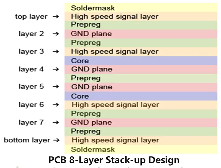
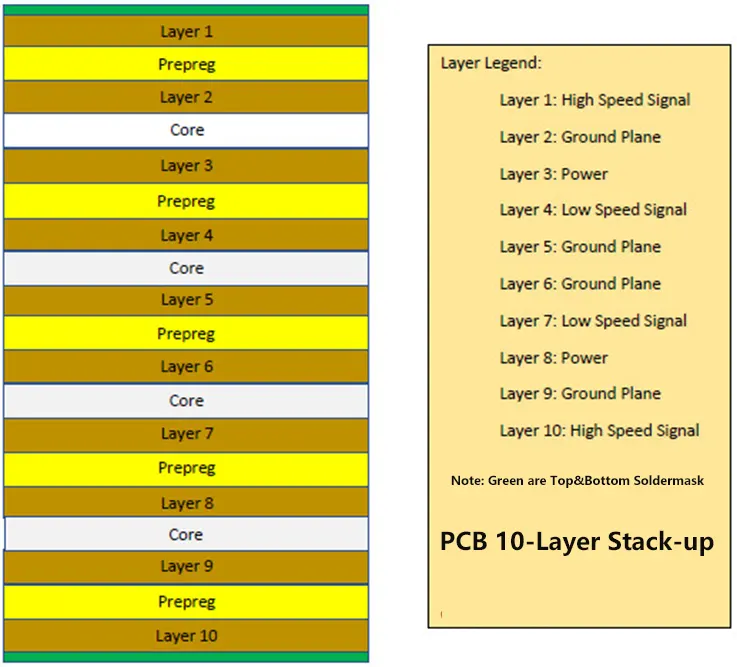
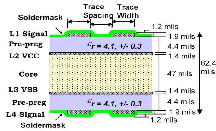
General layers in multilayer PCBs include the ground plane (GND plane), power plane (PWR plane), and inner signal layers. An example of an 8-layer PCB stackup is shown below.
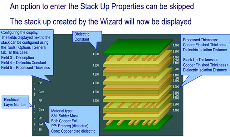
In PCB design, the distribution of layers in a printed circuit board follows a symmetrical or balanced structure, as depicted in the diagram. Alongside the layer distribution, it is also crucial to consider the spacing between layers. To achieve miniaturization goals, trace spacing must be minimized during the layer stack-up planning process. The interlayer space can comprise either core or prepreg materials. When fabricating multilayer PCBs, one or more cores and prepregs can be used.
The cores consist of copper-plated glass-reinforced epoxy laminate sheets, with thicknesses ranging from 0.1mm to 0.3mm. PCB design engineers must take into account these factors and carefully select core and prepreg materials with the appropriate thicknesses and interlayer spacing to improve signal integrity, reduce noise, and enhance various other PCB performance metrics. Proper layer stack-up planning is vital to ensure that the PCB is optimized for efficient signal transmission and high reliability.
PCB Stackup DesignRules and Considerations
The design and construction of a PCB layer stackup has a significant impact on the board’s production and assembly. During the fabrication process, it is crucial to consider key factors such as the number of layers and their layout, as well as the type of materials used. These considerations enable a balance between thickness constraints, material parameters such as coefficients of thermal expansion, dielectric constant, electrical strength, and signal isolation.
It’s important to carefully select the appropriate through-routing option, as it can impact the overall stackup design. PCB designers must be mindful of the various parameters that influence stackup design to ensure optimal performance and reliability. Understanding these factors is essential in creating an optimized PCB layer stackup, which can result in efficient signal transmission, while also limiting noise and EMI issues. Therefore, PCB designers must pay close attention to these aspects to create a highly-functioning printed circuit board.
● Number of Layers: When planning your printed circuit board (PCB) stackup, the first factor to consider is the required number of layers. This decision should be based on factors such as the type of signals (high-speed, low-speed), power demands (high-power boards or circuits utilizing power supplies), and ground layers or planes. It is strongly recommended to avoid mixing different types of signals on inner layers. For most boards, the layer count can be calculated using the pin density.
Once the pin density has been determined, it is advisable to consult your contract manufacturer (CM) for stackup support or refer to a readily available lookup table to determine the number of signal layers and the total number of layers required. Additional information, such as the values for controlling impedance, may also be required.
By thoroughly considering these factors and leveraging the expertise of your CM or utilizing reliable lookup tables, you can achieve a well-optimized PCB stackup that meets your design requirements and ensures optimal performance.
● The number of Signal Layers: In the design of printed circuit boards, the number of signal layers required can depend significantly on the intended application of the board. For example, high-speed signal or high-power applications often require more signal layers than low-speed signal applications.
When designing complex devices with a low pitch and a large number of pins, such as ball grid arrays (BGAs), it may be essential to use additional signal layers to accommodate the increased number of required connections.
Stringent signal integrity requirements, such as extremely low crosstalk, may also necessitate an increase in the number of signal layers to ensure optimal performance.
For mixed-signal applications, the separation of analog and digital signals is typically required, which often results in an increased number of signal layers.
During the design phase, the use of a signal and power layer estimation tool can be invaluable in determining the precise number of signal layers required to meet specific design requirements. By leveraging these tools, design engineers can allocate signal layers effectively and fine-tune their circuit board designs to optimize performance and functionality.
● The Number of Power and Ground Layers: Designers can employ ground and power planes to allocate certain signal layers exclusively for routing signals. These planes also help to minimize DC resistance in the power and ground rails, leading to a reduced DC voltage drop at the devices.
The ground layer refers to the copper plane connecting to the ground connector of the power supply. On the other hand, a power layer is a flat copper plane joined to the power supply rail.
Furthermore, these planes act as high-frequency and time-varying signal return pathways, reducing noise and signal crosstalk and promoting signal integrity. Power planes also improve the circuit’s capacitive decoupling capability, reduce electromagnetic radiation, and enhance electromagnetic compatibility (EMC) performance. By leveraging these benefits during the printed circuit board design process, designers can optimize the circuit’s reliability and performance.
● Controlled Impedance Traces: A controlled impedance trace is a circuit board trace and related planes that create the characteristic impedance of a transmission line. Achieving a uniformly managed impedance is crucial for preserving signal integrity.
In cases where the reference plane is not present on the adjacent layer, another copper feature located on that layer may serve as the reference.
During the manufacturing process, it is necessary to ensure a homogeneous etch across the length of the line, including the breadth and trapezoidal effect. To meet these requirements, etching tolerances must be maintained and consistency in the etching process is critical. By paying close attention to these details, designers can achieve optimal manufacturing outcomes, resulting in a printed circuit board design that performs efficiently and reliably.
● Spacing Between The Layers: In printed circuit board design, it is crucial to maintain a close coupling between the signal and current return planes to reduce capacitance. The coupling between ground and power planes should also be maintained at a close proximity.
Regardless of which adjacent plane they occupy, signal layers must always be situated near one another. Achieving tight coupling and a suitable layer spacing is necessary for ensuring continuous signaling and overall operational efficiency. It is advisable for designers to adhere to these principles during the layout to optimize the performance and functionality of the printed circuit board.
● Trace Width and Spacing: The routing of ball grid array (BGA) packages presents a significant challenge to PCB layout. During the design process, designers must pay close attention to the breakout area and determine the number of signals that require routing between vias. This crucial step establishes the minimum trace width and spacing that should be employed.
It is of vital importance to ensure that a minimum line width is observed to avoid any potential negative impacts on signal quality. PCB designers should carefully examine the design to check for any detrimental effects that may arise with narrow trace widths and make necessary adjustments. By following these guidelines, designers can effectively address challenges associated with routing BGA packages, thereby optimizing the design of the printed circuit board.
● Layer Arrangement: When designing a printed circuit board, determining the number of layers is a crucial first step. After that, it is necessary to establish how the layers should be stacked or ordered. Here are some good ground principles to follow:
● Route high-speed on minimum thickness microstrips.
● Avoid having two signal layers adjacent to each other.
● Place signal layers next to internal power layers for tight coupling.
● Make the stackup symmetric from the top and bottom layers inward.
● Power and ground layers should have minimal spacing between them.
When designing a printed circuit board, an essential aspect of stack-up architecture is the placement of sequential layers. Before routing, designers must carefully consider the arrangement of high-speed signal layers, with placement according to microstrip thickness being a crucial element. Signal layers are often situated close to the ground or power plane, leading to tight coupling.
In addition, limiting the number of lamination steps in sequential lamination plays a critical role due to the potential for increased costs and time consumption. PCB designers must maintain a good balance between stack-up complexity and cost-effectiveness to produce an optimal board design that meets performance, reliability, and fabrication requirements.
● Determining Layer Material Types: When designing a printed circuit board, selecting materials for the layer stackup is a critical aspect that requires consideration of their thermal, mechanical, and electrical properties, as well as how they interact with one another. For signals, 0.5-ounce copper is typically employed, while 1-ounce copper is used for power planes, and 2-ounces of copper may be used for high-current applications.
Typically, printed circuit boards feature a solid fiberglass substrate core that provides the PCB with thickness and strength. Some flexible PCBs, on the other hand, may use a flexible high-temperature plastic.
The next layer in the stackup consists of a thin copper foil that is affixed to the board. In double-sided PCBs, copper is found on both substrate sides, with the thickness of the copper varying depending on the layering of the PCB stack.
A solder mask layer is applied over the copper foil to prevent the copper traces from coming into contact with other metals. This layer is crucial in aiding users in soldering to the correct location while avoiding solder jumpers.
The silkscreen layer is applied over the solder mask layer to include symbols, numbers, and letters, making it easier for humans to understand the board and facilitate assembly. PCB designers must carefully select each of these components, ensuring they are sized appropriately and function optimally, for an optimized printed circuit board.
● Determining Routing and Vias: When designing a printed circuit board, it is important to route high-speed signals on intermediary layers located between levels. This design practice enables ground planes to act as a shield, effectively containing radiation produced by fast-moving signal tracks.
When signal levels are placed in proximity to plane levels, nearby planes are able to conduct the return current, reducing the return path inductance to a minimum. With standard construction techniques, it is possible to achieve decoupling below 500 MHz, thanks to the insufficient capacitance between adjacent power and ground planes.
High-speed signals are prone to signal integrity issues, and therefore, thorough consideration must be given to PCB design principles. By keeping these aspects in mind, designers can ensure effective signal transmission, reduce noise, and enhance the reliability and performance of printed circuit boards.
Recommendations in DesignPCB stack-up
To achieve an optimal printed circuit board (PCB) stack-up design, several best practices should be followed. Firstly, it is recommended to limit the number of sequential layers to three or fewer to reduce processing time and keep costs and delivery times under control.
When using stacked vias, they should be filled after each sequential layer, which can add complexity to the manufacturing process and increase the build-up’s span. Therefore, using staggered vias can be a cost-effective alternative if the design permits.
It is crucial to know the specific layers in which mechanical buried vias will be implemented and to determine the need for staggered and buried vias. This information must be carefully considered during the stack-up design phase.
It is also worth noting that sequential lamination may not be suitable for all materials. As such, manufacturers should verify the suitability of their materials for sequential lamination during the planning stages to avoid any potential issues during manufacturing.
By following these guidelines, you can design a well-optimized PCB stack-up that is technically sound and exhibits excellent manufacturability, ensuring a successful outcome for your PCB project.
PCB Stackup Design Example
Several PCB stack-up options can be accomplished depending on how you apply the tips mentioned earlier. This reference graphic demonstrates an exemplary 10-layer PCB stack-up design that is particularly useful in PCB design projects.
In modern circuits with high operating speeds, effective PCB stack-up design is critical to optimize distribution capabilities while minimizing interference. Poorly designed PCBs can significantly impact signal transmission, manufacturability, power delivery, and long-term reliability.
Multilayer PCBs offer extensive opportunities for creativity and can fully realize the potential of electronic circuits. Therefore, it is wise to entrust the design process to reputable companies that specialize in producing high-quality electronic products.
By engaging reliable design companies, design engineers can be assured of technically sound PCB designs that meet their specific requirements, including optimized stack-up configurations that meet the needs of high-speed circuits. These design firms have the expertise and best practices necessary to produce PCBs that provide excellent manufacturability, functionality, and reliability over the product’s lifetime. Ultimately, this approach can lead to high-quality electronic products with excellent performance and longevity.
Common PCB Layer Stack-Up Configurations
There are several common PCB layer stack-up configurations, including:
● 2-Layer PCB Stack-Up: Consists of two layers of copper, separated by a substrate material. This is the simplest type of PCB and is often used for low-speed or low-complexity circuits.
● 4-Layer PCB Stack-Up: Consists of two internal signal layers and two power/ground planes, separated by substrate layers. This is a common layer stack-up for complex, high-speed PCBs.
● 6-Layer PCB Stack-Up: Consists of two internal signal layers, two power planes, and two ground planes, separated by substrate layers. This stack-up is commonly used for high-speed or mixed-signal PCBs.
● 8-Layer PCB Stack-Up: Consists of four internal signal layers and two power/ground planes, separated by substrate layers. This stack-up is commonly used for very complex, high-speed PCBs.
● 10-Layer PCB Stack-Up: Consists of six internal signal layers and two power/ground planes, separated by substrate layers. This stack-up is commonly used for extremely complex, high-speed PCBs with multiple high-speed interfaces.
The exact layer stack-up used for a PCB depends on the specific requirements of the circuit and the system it is a part of, as well as any manufacturing or cost considerations.
Summary
Careful PCB Design Is Important!
In today’s high-speed circuits, exceptional PCB design is essential and has become an art form in its own right. Poorly designed printed circuit boards can lead to decreased electrical performance with respect to signal transmission, power delivery, producibility, and long-term reliability, negatively affecting the final product.
Submission of Gerber files to PCB manufacturers establishes production costs, where the cost per unit progressively decreases with increasing quantity. The surge in the usage of multilayer and flexible PCBs is driving the global expansion of the PCB industry. As electronics companies try to add more functionality to their devices, board density and design complexity continue to increase. For most consumers, the most critical factors for selecting a PCB manufacturer are price, quality, delivery time, and service, with price often being the primary consideration.
At JarnisTech, we are committed to reducing lead times during the critical prototype phase. By providing fast quotes in just 10 minutes and delivery lead times as short as 5 working days, we offer our customers greater peace of mind when it comes to their PCB manufacturing and prototyping needs. Our goal is to empower our customers with high-quality, reliable, and timely PCB manufacturing services that meet their specific requirements and help them achieve their business goals.
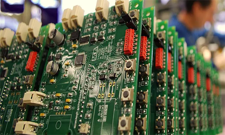
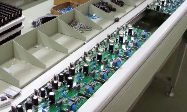
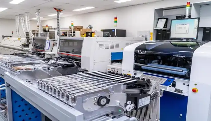
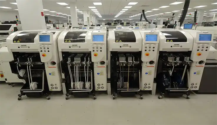
For any electronic manufacturing company, the utilization of turnkey printed circuit board assembly services is crucial to their function. Therefore, it is essential to identify an appropriate business partner who can fulfill your manufacturing requirements. JarnisTech offers turnkey PCB assembly services that enable you, the customer, to focus on the design and development of your exclusive product lines, while we handle the specifics of assembling them. This allows you to concentrate on other essential aspects of your business. We not only oversee the complete material procurement process, but we also handle the entire printed circuit board assembly process.
With four manual placement lines and four high-speed assembly lines, our business is suitably equipped to cater to diverse assembly requirements. Whether your project involves high-volume production of standard PCB assembly or advanced engineering for unique PCBA prototypes, JarnisTech can provide your company with the effectiveness and innovation that your products deserve.
Definition of PCB Assembly
Printed Circuit Board (PCB) Assembly is the process of mounting and soldering electronic components onto a PCB. It involves several stages, including component placement, soldering, and inspection, and is a critical step in the development of any electronic device, from simple circuit boards to complex systems. PCB Assembly can be done manually or with the help of automated machinery, depending on the scale and complexity of the project. The assembly process can be divided into two main categories – Full Turnkey and Partial Turnkey – each with its own benefits and limitations. Ultimately, choosing the right PCB Assembly method and service provider is crucial for ensuring high-quality, reliable electronics.
What Is Turnkey PCB Assembly ?
For PCB design engineers, the term “turnkey” when referring to printed circuit board (PCB) assembly denotes a product or service that is readily available for immediate use by the buyer. In the context of PCB assembly, this term indicates that the provider will handle all aspects of the project, including the procurement of parts and components, as well as the production of PCBs. Turnkey PCB assembly is a process that leverages internet-based cloud software and PCB manufacturers to develop printed circuit boards for small businesses. This method is known for its speed, efficiency, and cost-effectiveness.
In essence, opting for a full turnkey solution enables PCB design engineers to focus on designing PCBs, while allowing the provider to manage all other aspects of the project. The utilization of turnkey solutions can streamline the assembly and testing of circuit boards for products, thereby saving time and money. Furthermore, businesses can acquire printed circuit boards in the shortest possible time with turnkey solutions. A comprehensive turnkey PCB assembly service includes all the necessary services, including PCBA, required to build finished goods. These may include, but are not limited to, the following:
● PCB prototypes. ● High volume PCB assembly. ● Box build. ● Management of Inventory. ● Shipment to clients
Aspects That Make Turnkey PCB Assembly Services Beneficial
● Quick Turnaround Times: In a turnkey PCB assembly service, all the steps involved in the process are carried out under the same roof, which results in a greatly reduced turnaround time. When multiple suppliers are utilized, particularly if they are located in different countries, a substantial amount of time is often consumed in the process of communication and shipment. The consolidation of all the necessary services in a turnkey PCB assembly solution leads to a faster production timeline, ultimately allowing for quicker delivery of the completed product to the customer.
● Competitive Prices: Opting for a turnkey PCB assembly service eliminates the need to send raw PCB boards and electronic components to an assembly facility, reducing the financial burden associated with shipping. Turnkey PCBA service providers generally have a trustworthy supply chain in place, allowing them to acquire components at a substantially lower rate than the market average. The incorporation of procurement services into their turnkey assembly offering, enables them to leverage economies of scale and optimize production, thereby passing the cost savings onto the customer.
● Better Process Management: A dependable PCB assembly partner possesses the capability to closely monitor every facet of the process, commencing from the procurement of components to the production and finally, the testing phase. Their expertise enables them to stay fully informed about the status of each stage, allowing them to identify any potential issues early on and take appropriate corrective measures. By doing so, they can execute the project in a more efficient and seamless manner.
How Many Types for Turnkey PCB Assembly ?
Turnkey PCB assembly services can be categorized as partial or full depending on the extent to which the third-party provider is involved in the assembly process.
Basics of Full Turnkey PCB Assembly
Full Turnkey PCB Assembly is a comprehensive service that involves the assembly of a complete PCB, from component procurement to final testing and inspection. This means that the PCB supplier manages the entire process, from selecting and purchasing electronic components and PCB fabrication to assembly, testing, and delivery. The supplier is responsible for ensuring that all components and materials are of the highest quality, and that the final PCBs meet all specifications and requirements.
The full turnkey method eliminates the need for the customer to manage multiple vendors or contractors, as the PCB supplier handles everything from start to finish. This approach is ideal for customers who do not have the time, resources, or expertise to manage the PCB Assembly process themselves. Additionally, full turnkey PCB Assembly offers faster turnaround times, improved quality control, and lower overall costs compared to other methods.
Some of the benefits of full turnkey PCB Assembly include:
● Reduced lead times and fast delivery. ● Consistent quality control throughout the entire process. ● Lower overall costs due to bulk purchasing power. ● Increased production efficiency. ● Single point of contact for all aspects of PCB Assembly.
However, some of the drawbacks of full turnkey PCB Assembly can include limitations on component choices and potential loss of control over the assembly process.
Benefits of Full Turnkey PCB Assembly
Full Turnkey PCB Assembly offers several benefits over other PCB Assembly methods. Some of these benefits include:
● Faster Turnaround Time: With full turnkey PCB Assembly, the entire process is handled by a single supplier, which helps to streamline the process and reduce lead times, resulting in faster delivery times.
● Single Point of Contact: By working with a single supplier for the entire PCB Assembly process, customers have one point of contact for all aspects, from component selection to final testing and delivery.
● Improved Quality Control: The supplier is responsible for ensuring that all components are of high quality and that the final product meets all specifications and requirements. This results in consistent quality control throughout the entire process.
● Lower Overall Costs: With full turnkey PCB Assembly, suppliers can take advantage of bulk purchasing power for components and materials, resulting in lower unit costs for the customer.
● Increased Production Efficiency: Full turnkey PCB Assembly allows for greater production efficiency as the entire process is managed by a single supplier, resulting in reduced downtime and improved overall efficiency.
Limitations/Drawbacks of Full Turnkey PCB Assembly
While full turnkey PCB Assembly has many benefits, there are also some drawbacks to consider:
● Limited Component Selection: Because the supplier is responsible for procuring components, customers may have limited options for components compared to other methods where they purchase their own components.
● Reduced Control Over the Process: With full turnkey PCB Assembly, customers may have less control over the process as it is managed by the supplier. This can result in reduced flexibility, and potentially fewer options for customization or changes.
● Higher Upfront Costs: Full turnkey PCB Assembly requires customers to pay for the entire PCB Assembly process upfront, which can be a significant investment for some customers.
● Dependency on the Supplier: Customers who rely on full turnkey PCB Assembly may develop a dependency on their supplier, potentially making it more difficult to switch to different suppliers in the future.
Basics of Partial Turnkey PCB Assembly
Partial Turnkey PCB Assembly is a PCB Assembly method where the customer supplies some or most of the electronic components, and the supplier provides the remainder of the components and handles the PCB Assembly process. In partial turnkey PCB Assembly, customers typically supply high-value components such as microcontrollers or custom integrated circuits while leaving the rest of the components to the supplier.
The supplier is responsible for managing the assembly process, including PCB fabrication, component procurement, assembly, testing, and inspection. Partial turnkey PCB Assembly is a more flexible option than full turnkey as it allows customers to supply some of their components without having to manage the entire process.
Partial turnkey PCB Assembly is ideal for customers who have unique or specialized components that they want to use in their PCB but do not have the resources or expertise to handle the entire assembly process. This approach offers a good balance between flexibility and cost-effectiveness, as customers can save money by providing their expensive components and leaving the rest of the assembly process to the supplier.
Benefits of Partial Turnkey PCB Assembly
● Flexibility: Customers can choose which components they want to supply and which ones to leave to the supplier, giving them more control over the process.
● Cost-Effective: Customers can save money by providing their high-value components while still benefiting from the supplier’s bulk purchasing power for the remaining components.
● Reduced Lead Time: By working with a PCB Assembly supplier, customers can benefit from faster lead times and delivery than if they handled the process in-house.
● Quality Control: The supplier is responsible for ensuring that the final product meets all specifications and requirements, resulting in consistent quality control throughout the process.
Limitations/Drawbacks of Partial Turnkey PCB Assembly
While partial turnkey PCB Assembly has many benefits, it also has some limitations and potential drawbacks to consider. These include:
● Limited Component Selection: Customers still may have limited options for components compared to other methods where they purchase their own components. Also, there may be compatibility issues between the customer supplied components and the remaining components assembled by the supplier.
● Reduced Control Over the Process: Customers may not have complete control over the entire assembly process, potentially leading to reduced flexibility or customization options.
Higher Upfront Costs: Partial turnkey PCB Assembly requires customers to pay for both the supplier provided components and their own components, which can be a significant investment for some customers.
● Increased Complexity: By combining customer supplied components with supplier supplied components, the PCB Assembly process can become more complex, increasing the risk of miscommunications or errors.
● Dependence on the Supplier: Customers who rely on partial turnkey PCB Assembly may still develop a dependency on their supplier, potentially making it more difficult to switch to different suppliers in the future.
Comparison between Full and Partial Turnkey PCB Assembly
Full and partial turnkey PCB assembly differ in terms of the level of involvement of the service provider in the manufacturing process. Here’s a brief comparison between full and partial turnkey PCB assembly:
● Cost: Full turnkey PCB Assembly can be more expensive than partial turnkey, as the supplier provides all components. Customers should determine the cost-effectiveness of each method based on their component needs and their budget.
● Lead Time: Full turnkey PCB Assembly can have faster turnaround times since the supplier handles all aspects of the assembly process. But partial turnkey assembly may still offer quick delivery times compared to in-house assembly.
● Component Selection: Partial turnkey PCB Assembly allows customers to have more control over the components used in their PCB since they provide some or most of them.
● Control over the Process: Full turnkey PCB Assembly may provide less control for customers who want complete oversight over every aspect of the assembly process. Partial turnkey assembly could provide more control to the customer.
● Supplier Expertise: Customers who rely on partial turnkey PCB Assembly can benefit from working with a supplier who has experience in the assembly process and can provide additional expertise. Full turnkey can provide a larger range of supplier expertise as they handle all of the assembly.
Ultimately, the decision between full or partial turnkey PCB Assembly will depend on the project’s specific requirements and the customer’s priorities. Customers should consider the above factors when determining which assembly method will best meet their needs for cost-effectiveness, time efficiency, control, flexibility, and supplier expertise.
Factors to Consider When Choosing a PCB Assembly Service Provider
Selecting a PCB Assembly service provider involves assessing various factors. Some important factors to consider include:
● Quality and Reliability: The provider’s reputation for quality, reliability, and product consistency is a critical consideration. The service provider should have strict quality control measures, use quality components, and follow standard industry practices.
● Experience and Expertise: The service provider’s range of experience, years of operation, technical knowledge, and expertise can significantly impact the project’s success.
● Capability and Capacity: The service provider’s equipment and production facilities should be modern and sophisticated to handle PCB Assembly projects successfully. The service provider should also have the capacity to manage various project sizes, production runs, and customer requirements.
● Cost and Pricing: The PCB Assembly service provider’s pricing structure should be competitive and offer value for money. The provider should also be transparent about the cost elements, including additional charges in the future.
● Lead Time: The service provider should have the ability to deliver a product within the desired lead time. The provider should have considerable capability to execute a project efficiently, manage the supply chain, and implement best practices.
● Customer Service and Support: The service provider should offer customer support and be responsive, accommodating, and communicative in addressing concerns.
● Certifications and Standards: The service provider should comply with industry certifications and standards such as ISO9001, IPC-A-610, and RoHS.
● Flexibility and Customization: The PCB Assembly service provider should offer various assembly customization options such as quick turn-around time, special testing, and customized packaging.
JarnisTech takes pride in catering to a diverse range of industries, such as Industrial, Communications, Medical, Wearable Devices, IoT, Navigation System, Bio-robotics, Monitoring System, Aviation, LED Lighting, and many others. Our unwavering commitment to meeting the unique specifications, quality standards, cost considerations, and delivery timelines of our individual customers sets us apart.
Our PCB manufacturing and assembly manufacturing facilities are situated in Shenzhen, and we adhere to stringent international standards, including ISO 9001, RoHS, IPC-A-600, and IPC-A-610, to ensure that every single printed circuit board assembly meets both the environmental and regulatory requirements and the highest quality standards. Furthermore, the final stages of production – the manufacture of PCBs and PCBAs in our SMT facility – reflect our dedication to customer satisfaction.
As a result, By considering these factors when choosing a PCB Assembly service provider, customers can ensure that they work with a provider who has a reputation for quality, expertise, and reliable delivery and can meet specific project requirements within budget.
Why Choose JarnisTech ?
When outsourcing your end-to-end PCB assembly to a reputable service provider like JarnisTech, you can focus on your core competencies while benefiting from reduced costs and faster time to market. Our comprehensive services include material sourcing, design, manufacturing, and supply chain management, allowing us to fulfill all your requirements and help you reach your customers quickly.
Our turnkey electronic manufacturing services cover the entire production process, starting from material acquisition to final assembly. By taking care of all aspects of production, including design, procurement, assembly, and supply chain management, we can provide a hassle-free and efficient service to our clients.
Our services are tailored to meet the specific requirements of each client, allowing them to save time and money in the production of their products. By leveraging our expertise and experience in electronic manufacturing, we can help our clients optimize their designs, reduce their production costs, and bring their products to market faster.
Here is a rundown of what our turnkey electronic manufacturing services entail, as well as an explanation of how you can make use of them to cut down on the amount of time and money spent constructing your product:
● Complete Bill of Materials: As a reliable production partner, we understand the significance of creating and keeping track of the Bill of Materials (BOM) for every product development process. We acknowledge the time and resources involved in this vital function, and therefore, we take on the responsibility of creating and monitoring the BOM. Our team is committed to ensuring that your project schedule stays on track while performing a range of activities such as rapid and cost-effective sourcing of components and managing resources in sync with the production process to avoid delays.
We offer exceptional part procurement services that enable you to obtain high-quality Printed Circuit Board (PCB) components at the best possible prices that suit your budget. We assure you of superior output quality by maintaining consistent and open communication channels throughout the production process. We value your valuable time and offer quick quotations in as little as four hours, and you can expect quick delivery within 24 hours of your order placement. By choosing us as your PCB manufacturer, you can start your projects faster and with greater efficiency.
● Expert Services of PCB Layout: As a manufacturer, nothing can be more detrimental than the cost of rework and production delays. To mitigate such risk, we offer manufacturing feasibility evaluations that can assess the viability of your designs and help you stay on schedule to bring your product to market without any delay. Our team works forward-thinking to ensure that your designs are converted into an end product that is fit for sale by leveraging the latest cutting-edge technologies such as PADS, Altium, and Cadence.
By our manufacturing feasibility evaluations, you can be assured that your design will be reviewed and evaluated against our extensive industry experience and knowledge. This service also enables you to identify any potential roadblocks early in the design process and determine the most efficient and cost-effective manufacturing solutions. With our focus on delivering high-quality results, we ensure that your product development process stays on track and avoids unnecessary delays, which ultimately leads to improved market competitiveness.
● Solutions of Customized PCB Assembly: Our organization is an industry-leading provider of circuit board assembly services and has significant experience delivering customized solutions that cater to the most challenging requirements and timeframes.
Our expertise in PCB assembly is hard to match, and we are always ready to accommodate your specific manufacturing needs as per your schedule and budget. We have a team of highly skilled professionals whose creativity and innovation allow us to deliver custom solutions that meet your unique demands.
We understand the importance of timely delivery in today’s rapidly evolving business world, and thus we have streamlined our processes to ensure that we deliver on time regardless of the complexity of the project or the deadline. Our commitment to quality is second to none, and we leverage modern technologies and techniques to ensure the reliability and durability of our PCB assemblies.
● Stringent of Testing Procedures: As a professional Printed Circuit Board (PCB) manufacturer, we fully comply with industry and regulatory standards and have implemented rigorous quality control procedures to meet the ISO-9000 and ITAR certification requirements.
Our quality control procedures are designed to ensure that each circuit board is manufactured and tested to function accurately and reliably. We conduct extensive testing and inspection at every stage of the production process to identify any potential defects, faults, or errors that could compromise the performance of the PCB.
We firmly believe in adhering to internationally recognized industry standards, and our quality control policies help us ensure that your circuit boards are manufactured and tested to the highest standards. Our commitment to quality is reflected in our strict adherence to all applicable regulatory and environmental standards.
● Quality Control of PCB Assembly: As a professional Printed Circuit Board manufacturer, we are committed to maintaining the highest standards of quality and reliability in every aspect of our operations. We follow the IPC-A-610 requirements meticulously during the assembly of all bare PCB boards to ensure that our products meet industry and customer standards.
Our team consists of highly experienced and skilled technicians and inspectors who have the expertise to handle every aspect of the PCB manufacturing process. We handle all aspects of the manufacturing process in-house, which enables us to ensure compliance with IPC Class II or III standards based on the customer’s needs.
We ensure that every bare PCB is subjected to comprehensive electrical testing, using either a flying probe or a fixture, to ensure accuracy and reliability. We follow a 100% visual examination process after the electronic PCB assembly is completed. For further assurance, we offer an optional 100% functional test performed in accordance with documented test procedures.
Our commitment to quality goes beyond the manufacturing process. We ensure that every finished PCB is cleaned 100% to remove any dust or debris that might affect its performance. We also enforce strict controls on electronic static discharge (ESD) to prevent any chance of damage to the PCB.
Therefore, partnering with JarnisTech for turnkey electronic manufacturing services means that our clients can concentrate on their core strengths, while benefitting from cost savings and faster time to market. Our comprehensive services cover the entire product life cycle, ensuring that our clients’ requirements are met efficiently and effectively
Turnkey PCB Assembly: Files Requirement
● Gerber or ODB++ Files: Copper, solder mask, silkscreen, solder paste, outline, thru-via hole, blind and buried via, micro-via, carbon ink printing, FPC stiffener, EMI film, and any other layers necessary should be included.
Excel version of the Bill of Materials (BOM) document. Your BOM ought to contain the following:
● Description (optional). ● Manufacturer (optional). ● Quantity per board (required). ● Reference designators (required). ● Manufacturer part number (required). ● Package (QFN32, SOIC, SOT23-5, 0402, etc.) (optional). ● Type (SMD, Thru-Hole, Fine-Pitch, BGA, etc.) (optional). ● IColumns indicating whether the parts were consigned by you, JarnisTech supplied, or not populated are highly desirable.
● Centroid File: The necessary file for PCB assembly is commonly referred to as the coordinates file, or the select and place file, and must be in CSV format. This file should include accurate component positions, rotations, and reference designators. Optionally, if a solder paste layer is included in the Gerber file package, Assembly Drawings may also be provided.
For complex PCBs, Assembly Notes can be incredibly useful during production, and can be saved in PDF format for convenience.
Tab routed, Breakaway tabs, V-scored and Routed + V scored
Rework:
BGA removal and replacement station, SMT IR rework station, and Thru-hole reworks station.
Design file format:
Gerber RS-274, 274D, Eagle and Auto CAD’s DXF, DWG BOM, and Pick and place a file
PCB Assembly Request For Quote
We are pleased to inform our valued customers that our team is readily available to address any inquiries or concerns related to order placement. At JarnisTech, we offer competitive pricing and direct savings pass-throughs to our customers who choose to purchase our full or partial turnkey PCB assembly services. To request a price estimate, we encourage customers to visit our RFQ page and provide the necessary information. Furthermore, our dedicated customer support staff can be reached at 0086-755-23034656 for additional assistance. For a comprehensive list of the required documents that must accompany the quote request, please contact us now.
Conclusion
When deciding between full and partial turnkey PCB Assembly, customers should consider their component needs, budget, control, and flexibility.
To choose a reliable PCB Assembly service provider, customers should conduct research and consider factors such as the provider’s reputation, experience, expertise, capacity, cost, lead time, customer service and support, and adherence to industry standards and best practices.
In short, taking the time to thoroughly evaluate PCB Assembly service providers and consider the necessary factors will help ensure that the chosen provider can meet your project requirements
In China, JarnisTech is a highly reputable and experienced PCB manufacturer that has been providing quality services to clients for many years. we offer a wide range of PCB manufacturing services, including turnkey and prototype assembly, PCB layout and design, and PCB fabrication. And if you want to know more and more, please contact us today.
The manufacturing process of PCBs is influenced by multiple factors, with the thickness being a key variable. The electrical conductivity and resistance of a PCB are significantly impacted by its thickness. Therefore, it is crucial for PCB manufacturers to carefully choose the appropriate thickness to ensure an optimal fit for a given application. Precision and accuracy in selecting the ideal thickness are essential for ensuring proper functionality and performance of the PCB.
Printed Circuit Boards (PCBs) are the backbone of modern electronic devices, serving as a platform for connecting and controlling various components on a circuit. Therefore, PCB thickness is a crucial factor in its design that can have a significant impact on performance, durability, and reliability. Different types of PCBs require distinctive thickness, and selecting the right thickness for your PCB is central to achieving optimal performance and longevity. In this article, we will provide an overview of standard PCB thickness, including the factors that impact it and how to choose the right thickness for your needs.
What Is PCB Thickness ?
PCB thickness refers to the overall depth or height of the printed circuit board. It is typically measured from the surface of the copper traces or planes on one side of the board to the surface on the opposite side. The thickness of a PCB affects its mechanical strength, electrical performance, and heat dissipation characteristics. Different types of PCB applications may have different requirements for thickness, and choosing the right thickness is important for ensuring optimum performance and reliability of the circuit board.
Many PCB contract manufacturers advertise 1.57mm or 0.062in as the standard PCB thickness. This reference is accurate to some extent, given that bakelite sheets were historically produced in this size during the early days of board fabrication. Consequently, this size has become the standard PCB thickness throughout history. Despite this standard, contemporary boards are available in varying sizes, both larger and smaller than the traditional 0.062in size. However, it is still widely accepted that 0.062in is the most common thickness for most designs.
In reality, there is now a range of common or standard PCB thicknesses available, including 0.031in (0.78mm), 0.062in (1.57mm), and 0.093in (2.36mm). Depending on the specific requirements of the job, custom-ordered boards with differing thicknesses can also be ordered from PCB manufacturers. PCB manufacturers must consider several factors during the design and manufacturing phase when determining the appropriate PCB thickness. The factors may include but not limited to:
Design Factors Influencing PCB Thickness
●Signal Types: The various signal types carried by PCBs have a direct impact on the selection of materials used for board production, and subsequently, the thickness of the board itself. For instance, PCBs that carry high power signals require thicker copper layers and wider traces, necessitating a significantly thicker board compared to low power signal boards.
Conversely, high-density PCBs that carry more complex signals tend to be thinner than other board types. This is due to the use of thin, high-performance materials and laser microvias, which allow for the creation of fine traces and higher density interconnections. PCB electronic engineers must be knowledgeable of these signal-specific board thickness requirements to select optimal materials and ensure efficient PCB design and development.
●Types of Vias: PCB vias play a critical role in the design process by routing traces through the-board, allowing for more compact and optimized designs. There are several types of vias available for such purposes, including:
The choice of via type and its density can impact the PCB thickness required to accommodate them. For instance, thinner boards can utilize micro vias due to their smaller size and ability to support high-density connections. In contrast, larger or more widely-spaced vias will likely require a thicker board to maintain acceptable structural integrity. PCB electronic engineers must consider these factors to determine the optimal board thickness, ensuring successful design implementation and functionality.
● PCB Board Materials: For PCB manufacturers, the materials utilized in the fabrication of a PCB play a crucial role in determining the operational performance and lifespan of the board, as well as its thickness. The typical construction of a PCB consists of substrate, laminate, solder mask, and silkscreen; however, substrate and laminate are of particular importance in relation to board thickness. Both substrate and laminate are responsible for providing the foundation and structure of the PCB and, therefore, impact its overall thickness significantly.
The substrate material used may differ depending on the dielectric constant required, with options including paper and epoxy resin, glass weave, or ceramic. Laminates are constructed using a thermoset resin layered with paper or cloth. Both substrate and laminate offer various configurations, significantly impacting the circuit board’s thermal, mechanical, and electrical properties, as well as its overall thickness. PCB manufacturers must consider the desired performance requirements when selecting the optimal material configuration, balancing design goals with practical considerations to ensure the highest quality and most efficient results.
●PCB Copper Thickness: In PCB manufacturing, the thickness of copper utilized plays a vital role in the determination of the board’s overall thickness. The copper layer thickness is typically determined based on the amount of current that must flow through the PCB. The standard copper thickness for PCBs is between 1.4 and 2.8 mils (1 to 2 oz). However, specific board requirements may necessitate adjustments to these standards.
As thicker copper layers require additional materials and imposing processing challenges, they translate into a thicker board, and ultimately, a higher production cost. With the copper thickness being a major determinant of overall PCB thickness, manufacturers must make informed decisions about copper layer thickness to meet performance requirements while maintaining practical and economic constraints.
● Number of PCB Layers: As a PCB design engineer, it is crucial to consider the number of layers required, as this will significantly impact the board’s thickness. Two to six-layer PCBs typically fall within the standard PCB thickness range, but eight-layer and higher PCBs may require a non-standard thickness. While it may be possible to achieve standard thickness by using thinner PCB layers, this becomes increasingly impractical as the number of layers increases.
In the event of a design requiring more layers, it is advisable to accommodate a thicker PCB. On the other hand, if a design must adhere to specific thickness parameters but doesn’t require multiple layers, reducing the number of layers is recommended. By considering such crucial factors, PCB designers can develop effective designs that meet requirements for performance, practicality, and cost-effectiveness.
●Operating Environment: As a electronic manufacturer, it is crucial to acknowledge that a PCB’s thickness and materials greatly influence its conductivity and resistance, making it critical to select an appropriate thickness for specific environments.
For instance, a thin or flexible board may not be the best option for challenging operational conditions. Similarly, designing thicker copper traces may not prove suitable for high-current or thermally variable environments due to limited thermal stability. It is imperative to carefully evaluate the material and performance requirements of the connectors and components on the PCBs in relation to the board’s thickness. This evaluation helps designers reasonably determine whether a standard or custom PCB thickness is preferable, depending on the operational requirements, practicality, and cost-effectiveness.
However, the design process does not end here; manufacturers must also play an active role in the process to discuss their capabilities and limitations and how these may impact the final PCB design. Effective collaboration between designers and manufacturers facilitates the development of high-quality PCBs that meet the desired performance requirements while remaining viable and cost-effective.
The Influence of PCB Thickness in the Manufacturing
●Layer Count: As a PCB designer, it is essential to recognize that more layers on a board can make it increasingly difficult to achieve a standardized thickness during manufacturing. While some specialty manufacturers may be capable of creating stacked PCBs with thinner layers to meet specific thickness requirements, this capability may not be universal and often comes with an associated cost increase.
It is imperative to consult with the manufacturer before finalizing the board design to gauge their capabilities and determine what they can achieve in terms of layering requirements. Conducting these discussions before finalizing the design helps identify and address any potential issues in advance, ensuring that the design meets all necessary specifications. Moreover, effective collaboration between designers and manufacturers helps deliver high-quality PCBs that achieve the desired performance goals while remaining practical and feasible in terms of manufacturing and costs.
● Copper Thickness: As a PCB manufacturer, it is crucial to acknowledge that etching is one of the most crucial steps in PCB fabrication for creating copper traces. The thickness of the internal copper layer directly impacts the etching and plating manufacturing processes. Consequently, thicker copper layers will have a notable impact on the overall PCB manufacturability, which can potentially affect the board’s design and production cost. It is therefore essential to consider the copper layer thickness during the initial design stage to ensure the chosen thickness meets the manufacturing process’ requirements and remains within the available budget.
By working closely with designers to evaluate copper thickness requirements, manufacturers can deliver high-quality PCBs that meet the necessary performance goals while remaining feasible and cost-effective.
● Drill Hole Equipment: As a PCB manufacturer, it is crucial to recognize that while drill hole size and spacing are vital considerations in achieving performance goals, drilling holes in PCBs introduces a new layer of complexity in the manufacturing process. Manufacturers face limits in drilling holes through the thickness of the board, which are determined by milling machines and lasers’ diameter and depth. This limit is represented by an aspect ratio, which is the ratio of the hole’s depth to the diameter of the drill hole. For standard drilling, all manufacturers should be able to achieve a 7:1 aspect ratio.
However, some manufacturers may achieve a higher aspect ratio, but this will raise the board’s cost and needs to be discussed with the manufacturer before finalizing the board design. Thicker boards can limit manufacturers’ ability to drill smaller diameter holes. By considering the aspect ratio limitations during the design stage, designers can develop an effective design that accommodates the necessary performance requirements while remaining practical and cost-efficient. Effective collaboration between designers and manufacturers further ensures the production of high-quality PCBs that match the desired performance profile.
●Depanelization Method: As a PCB manufacturer, it is critical to acknowledge that depanelization is another crucial manufacturing consideration. Typically, PCBs are fabricated on large panels containing several boards that are later separated to create individual boards. The thickness of the board influences the depanelization method utilized. For instance, thicker boards necessitate careful scoring, whereas thinner boards may be routed to create breakaway tabs. To optimize depanelization, it is vital to work closely with the manufacturer and discuss the various depanelization techniques as well as any unique depanelization requirements.
It is essential to engage the manufacturer in these discussions before completing the final PCB design since these manufacturing factors are dependent on the manufacturer’s capabilities, methods, and associated costs. Failure to discuss these elements earlier in the design process can result in modifications or complete redesigns of your layout, leading to additional costs. Therefore, PCB manufacturers must collaborate effectively with designers and provide critical input on manufacturing requirements to ensure a smooth production process that produces high-quality and cost-efficient PCBs.
Standard PCB Thickness Types
Standard PCB thickness can vary depending on the specific type of board and its intended application. Here are some typical thickness values for various types of PCBs:
●Single-layer PCB thickness: Between 0.4 mm and 1.6 mm.
●Double-layer PCB thickness: Between 0.8 mm and 2.4 mm.
These values are considered standard in the industry and are used by PCB manufacturers as a guide in the design and production of circuit boards. However, it’s essential to consider the specific requirements of each application to ensure the selected thickness is appropriate for the performance and reliability needed. Additionally, custom thicknesses may be required in unique cases, such as those with specific design constraints or unusual requirements for thermal management or structural support.
Considerations When Choosing PCB Thickness
Choosing the appropriate PCB thickness depends on various factors, such as the complexity of the circuit design, board size, component density, thermal management requirements, and mechanical constraints. Here are some factors to consider when selecting the right PCB thickness:
●Mechanical strength: If the PCB will be subjected to stress or external loads, it’s important to have enough thickness to ensure mechanical strength and avoid bending or breaking.
●Component density: High-density PCBs or those with large components may require thicker thickness to accommodate the component height and prevent interference between them.
●Thermal management: For applications with high power dissipation or significant heat generation, a thicker PCB can provide better thermal performance by allowing for more effective heat dissipation.
●Electrical properties: The thickness of the PCB can influence impedance, signal integrity, and electrical properties. It is critical to match the board thickness to the impedance. This is due to the fact that the thickness of the board is actually the thickness of the dielectric, and the dielectric aids in impedance control. Therefore, the selected thickness must meet the specified requirements of the circuit design.
●Cost and manufacturing: Thicker PCBs may be more expensive and require additional manufacturing steps that can affect the cost and time to manufacture the board.
●Equipment Capabilities: When manufacturing PCBs, it is critical to evaluate whether the manufacturer has the necessary equipment to achieve the desired board thickness. Moreover, if an application requires intricate features that can only be realized through advanced design techniques, it is crucial to identify manufacturers who can meet such requirements as early as possible.
However, such techniques generally come with added costs that need to be taken into account. By prioritizing a deep understanding of client requirements during the design phase, manufacturers can effectively match client needs with production capabilities, while also ensuring a cost-effective outcome. Effective collaboration between manufacturers and clients is essential in developing and delivering high-quality PCBs that accurately align with all specifications, such as performance, manufacturing, and budget.
Turnaround Time: In PCB manufacturing, standard thicknesses present minimal difficulties, and the production process requires very few adjustments. However, for custom thicknesses, adjustments are necessary, which can significantly increase production time. Adapting existing equipment settings and processes to fit the custom design requirements can be time-consuming and affect the manufacturing schedule, potentially delaying turnaround time.
If the design includes complex features, this will further increase the manufacturing time. Therefore, when considering a custom PCB thickness, it is crucial to engage with the manufacturer to obtain an accurate estimate of the time required for its production. By liaising with the manufacturer, clients can adjust their delivery timelines accordingly, preventing any uncertainty or delays. Collaborative communication between manufacturers and clients is essential in developing high-quality, custom PCBs that precisely match performance requirements while remaining feasible in terms of manufacturing time and budget constraints.
●Additional Cost: As experienced PCB engineers, it is crucial to carefully evaluate the cost-effectiveness of producing a custom circuit board for your company. Standard-thickness boards offer significant advantages, including reduced manufacturing costs and avoidance of potential delays associated with custom-thickness boards. Therefore, it is imperative to make a thorough analysis of the cost-benefit trade-offs before deciding on a custom-thickness board. While it is true that using special materials to accommodate a standard thickness may be more expensive, it could potentially outweigh the costs associated with modifying a custom-thickness board. It is essential to take all relevant factors into account and make a well-informed decision that aligns with your company’s goals and requirements.
So, selecting the right PCB thickness requires consideration of various factors that impact the performance, reliability, and manufacturing of the board. The selected thickness should meet the specific needs of the application while balancing design requirements, manufacturing costs, and other practical considerations.
Conclusion
PCB thickness standards vary according to the type of board and intended application, and custom thicknesses may be required in some cases. Ultimately, selecting the appropriate PCB thickness requires balancing the requirements of the intended application with considerations of manufacturing cost, design complexity, and other practical considerations.
It is evident in the PCB industry that PCB thickness plays a vital role in ensuring the necessary functionality of a printed circuit board. As PCB manufacturers, we understand this and strive to provide accurate results for the best performing PCBs to our esteemed clients.
We value every customer’s investment in purchasing a PCB and appreciate the trust bestowed upon us. Hence, we leverage our extensive experience and cutting-edge technology to design PCBs that adhere to our client’s specified standard thicknesses.
Should you have any questions about PCBs, PCB manufacturing, or the PCB assembly process for your project, our team is available to assist you 24/7. Most importantly, we take pride in delivering critical high-performance PCB and PCBA solutions to our clients’ doorsteps, ensuring their satisfaction every step of the way.
Printed Circuit Board (PCB) Assembly is the process of mounting electronic components onto a circuit board. PCBs are used extensively in the manufacturing of electronic equipment, and their assembly involves a combination of manual and automatic processes, such as soldering, inspection, testing, and more.
It is important to note that the PCB Assembly process is separate from the manufacturing of PCBs themselves, which includes design and prototyping. The actual assembly process involves the precise placement of Active and Passive Electronic Components onto the PCB, depending on the unique characteristics of the PCB and the specific application it is intended for.
The assembly of electronic components is therefore a crucial step in the overall PCB manufacturing process, requiring skilled technicians and specialized tools in order to ensure accurate and reliable assembly. PCB Assembly Manufacturers play a key role in this process, utilizing their expertise to produce high-quality, fully functional circuit boards that meet the needs of a wide range of modern electronic devices.
Introduction to Printed Circuit Board Assembly (PCBA)
Printed Circuit Board Assembly (PCBA) is the process of assembling electronic components onto a printed circuit board (PCB) to create a functional electronic device or product. The PCB is the foundation of most electronic products and acts as a platform for the placement and interconnection of electronic components. PCBA involves a series of steps that include solder paste application, pick and place of components, reflow soldering, inspection, and testing. The PCBA process requires specialized equipment, expertise, and quality control measures to ensure that the final product meets design specifications and is reliable and safe for use. The PCBA process has evolved over the years to become more automated and efficient, with advancements in technology leading to smaller, more complex, and higher density circuit boards.
The History and Evolution of PCBA
The history of Printed Circuit Board Assembly (PCBA) can be traced back to the early 20th century when simple radio circuits were constructed on thin sheets of Bakelite or Masonite material. In the 1940s, during World War II, the use of PCBs became prominent for military applications and by the 1950s, printed circuit boards became more widely used in commercial applications. The early PCBs were single-sided and used through-hole components.
In the 1960s, the use of surface-mounted components on PCBs was introduced, which allowed for the miniaturization of electronic products. As PCB technology advanced, the use of automated assembly equipment, such as pick and place machines, and reflow soldering ovens, became more prevalent in the 1980s, leading to increased production efficiency and reduced costs.
In the 1990s, the high-density interconnection (HDI) technology was developed, which enabled the integration of more components on smaller PCBs, paving the way for smaller and more powerful electronic devices such as smartphones and tablets.
Today, the PCBA industry continues to evolve, with advancements in technology enabling even more miniaturization, enhanced functionality, and increased reliability. The use of flex PCBs, rigid-flex PCBs, and 3D printing is becoming more widespread, and the introduction of the Internet of Things (IoT) has led to higher demand for smaller and more energy-efficient PCB assemblies. The trend towards smart manufacturing and Industry 4.0 is also driving the development of more automated and connected PCBA processes.
PCB Design and Layout Considerations
PCB design and PCB layout considerations are critical in Printed Circuit Board Assembly (PCBA) as they can affect the functionality, reliability, and manufacturability of the final product. Here are some key considerations:
●Component selection and placement: The placement of components on the PCB should be optimized for the best performance, thermal management, and ease of assembly. Components should also be selected based on their availability, cost, and performance requirements.
● Signal integrity and power integrity: The PCB should be designed to ensure proper signal integrity by minimizing noise, crosstalk, and signal reflections. Proper power delivery and distribution networks are also required to ensure power integrity.
●PCB stackup and layer count: The PCB stackup should be designed to minimize noise and crosstalk while optimizing signal and power integrity. The layer count should be optimized for the complexity of the circuit and the size of the board.
● Trace routing and spacing: The routing of traces on the PCB should be designed to minimize noise and EMI issues while optimizing signal integrity. Trace spacing should also be optimized for the required conductor width, voltage, and current.
●Thermal management: The design should ensure proper heat dissipation and thermal management to prevent issues such as overheating, component failure, and signal distortion.
● Design for manufacturability (DFM): The PCB design should be optimized for ease of assembly and cost-effective manufacturing.
●PCB testing: The design should allow for proper testing of circuits and components to ensure performance and reliability.
Therefore, PCB design and layout considerations are critical in ensuring that the final PCBA product meets performance requirements, is reliable, and can be manufactured efficiently and cost-effectively.
PCB Fabrication Overview
PCB fabrication is the process of manufacturing the Printed Circuit Board (PCB) that serves as the base for Printed Circuit Board Assembly (PCBA). The PCB fabrication process involves a series of steps, including the following:
●Design: The PCB design is created using PCB design software or other CAD tools.
● Substrate material selection: The substrate material for the PCB is selected based on the requirements of the circuit. Common substrate materials include FR-4, polyimide, and Rogers laminates.
●Copper layer formation: Copper is deposited onto the substrate material through a process called electroless copper plating.
●Photolithography: A photoresist layer is applied to the copper layer, and a pattern is created with the use of a photomask. The copper layer is then etched to remove excess material using a chemical process.
● Drilling: Holes are drilled into the PCB to create the required vias and through-holes.
●Plating and solder mask application: Additional copper plating is applied to the PCB, followed by the application of a solder mask to protect the copper layers and to indicate the location of solder pads.
● Silkscreen printing: A layer of ink is applied to the board’s surface using a silkscreen process to print component labels, logos, and other markings.
●Electrical testing: The PCB is subjected to electrical testing to ensure that it meets design specifications and is free from defects.
PCB fabrication is a complex process that requires specialized equipment and expertise. The quality of the PCB is critical to the performance and reliability of the final product. Additionally, advancements in PCB fabrication technology have led to the development of new substrate materials, more precise manufacturing processes, and increased fabrication efficiency.
PCBA Process Flow
The PCBA process flow involves a series of steps that transform a printed circuit board (PCB) into a functional electronic device or product. The typical PCBA process flow includes the following steps:
●Solder paste application: Solder paste is applied to the PCB surface using a stencil printing process or jetting.
●Pick and place of components: Automated pick and place machines are used to accurately place surface mount components onto the PCB. Through-hole components are typically placed manually.
●Reflow soldering: The PCB is heated in a reflow oven to melt the solder paste, forming a permanent solder joint between the components and the PCB.
●Inspection: Quality control checks are performed to ensure correct component placement, proper soldering, and any defects are identified and addressed.
●Testing: The assembled PCB is electrically tested to ensure it meets the required performance specifications and functionality.
●Rework and repair: If any defects or issues are identified during inspection or testing, rework and repair may be required to correct them.
●Final assembly: Additional components such as connectors, cables, and housings are added to the PCB to complete the final assembly of the electronic product.
Overall, the PCBA process flow requires specialized equipment, expertise, and quality control measures to ensure that the final product is reliable, safe, and meets the required performance specifications. Additionally, advancements in PCBA technology have led to the development of more automated and efficient processes, reducing production time and costs while increasing manufacturing yield and product reliability.
How Many Methods Are Needed To Make PCB Assembly ?
There are two major techniques that a PCBA manufacturer could employ for PCB assembly:
Surface-Mount Technology
Surface-mount technology (SMT) is a sophisticated assembly process that involves mounting electronic components directly onto the surface of a printed circuit board (PCB). This method is highly automated and flexible and enables manufacturers to achieve higher connection density and greater precision in the assembly of complex circuits.
By using SMT, manufacturers have the ability to incorporate intricate circuitry into smaller components. This is made possible by the precision placement of components directly onto the surface of the PCB, which eliminates the need for bulky mounting structures. The result is a more compact and efficient electronic device with improved performance and reliability.
SMT has become increasingly popular due to its many advantages, including greater flexibility, speed, and accuracy, which allows for an improved manufacturing process and higher quality end products. Manufacturers who utilize SMT assembly methods must have the necessary expertise and specialized equipment to ensure that all components are placed in the correct location, with the correct orientation, and with the appropriate level of bonding to create a fully functional electronic device.
● The PCB Is Prepared: First, the assembler puts solder paste in the areas it’s required on the board.
● Then, The Components Are Placed: Next, the assembler puts elements on the boards, typically with a pick-and-place machine.
● Reflow Soldering: The assembler heats the boards inside an oven for reflow till the paste has reached the temperature that is required for solder joints to be formed.
● Checking: The assembler conducts inspections throughout the SMT process, which includes prior to attaching components, and prior to and following the reflow soldering process.
Through-Hole Technology
The thru-hole technique is an assembly method that involves the drilling of holes in a printed circuit board (PCB) to allow for electronic components, referred to as leads, to be inserted and connected. This technique has been around for many years and is considered an older technology in comparison to surface-mount technology (SMT). Despite this, the thru-hole technique offers unparalleled durability and reliability due to the stronger connections created between the components and the board.
In the thru-hole assembly process, leads of components are inserted into corresponding holes in the PCB and then soldered to create a strong and reliable bond. This method can also accommodate larger components compared to those used in surface-mount technology.
Even though SMT has gained more popularity in recent years, the thru-hole technique is still commonly used in certain applications, especially for components that require higher mechanical strength and stability. Manufacturers with knowledge and experience in both SMT and thru-hole assembly methods are able to provide a wide range of options to meet the varied requirements of different electronic devices.
● Drilling Holes: The initial step in the process of drilling thru holes involves drilling holes in the board. The holes should be the proper dimensions for the component leads.
● Place The Leads In The Holes: Next, the assembly worker places the leads into the holes.
● Soldering: The subsequent step of the procedure is the process of soldering. This ensures that the components are held securely in their place.
● Inspect: Throughout the process, the assembly goes through checks to ensure that the PCBA is operating as intended.
Surface Mount Technology (SMT) vs. Through Hole Technology (THT)
Surface Mount Technology (SMT) and Through Hole Technology (THT) are two common techniques used in Printed Circuit Board Assembly (PCBA) to mount electronic components onto a printed circuit board (PCB). There are some key differences between these two techniques:
●Component packaging: SMT components are typically smaller and lighter compared to THT components, as they are designed to be mounted on the surface of the PCB. THT components, on the other hand, have leads or wires that are inserted through the holes in the PCB and soldered onto the other side.
●PCB Design: THT components require larger holes in PCBs to accommodate the leads, while SMT components only require small pads on the PCB surface. This can impact PCB design, especially when it comes to high-density boards with limited space.
●Assembly process: SMT components are typically assembled using automated pick and place machines, while THT components are inserted manually or using selective wave soldering machines. SMT components can be assembled at a quicker rate due to automation, while THT components take more time for assembly.
●Reliability: SMT components have less physical contact with the PCB, resulting in potential issues with vibration and shock resistance. THT components, being fastened through the board, have more mechanical strength.
●Cost: The cost of SMT components is often lower compared to THT components because they are smaller and lighter, and require fewer materials. However, SMT assembly processes can be more expensive due to the need for pick and place machines and reflow ovens.
Generally speaking, the choice between SMT and THT largely depends on the design specifications, production quantity, and intended application of the electronic product. SMT is currently the more popular choice due to its smaller size, higher assembly speed, and lower cost. However, THT is still used for certain applications, such as in high-power or high-vibration environments where added mechanical strength is required.
Key Components Used in PCBA
The key components used in Printed Circuit Board Assembly (PCBA) include:
●Resistors: Resistors are used to limit the flow of current in a circuit.
●Capacitors: Capacitors store and release electrical energy, stabilize power supply, and filter noise.
●Diodes: Diodes allow the flow of current in only one direction, typically used in rectification, voltage regulation, and signal processing.
●Transistors: Transistors are semiconductor devices that amplify or switch electronic signals in a circuit.
● Integrated Circuits (ICs): ICs are miniature electronic circuits that contain many electronic components such as transistors, diodes, resistors, and capacitors.
●Memory Devices: Memory Devices such as Flash memory, EEPROM, SDRAM etc. are used in electronic devices to store data and instructions.
●Microcontrollers (MCUs): MCUs are single chip microprocessors that contain all the basic components necessary for controlling a device or a system, including memory, processor, and input/output peripherals.
●Connectors and headers: Connectors and headers are used to establish electrical connections between PCBs, devices and external interfaces.
●Sensors: Sensors are used to measure physical variables such as temperature, pressure, and motion.
●Passive components: Passive components include ferrites, inductors, coils, transformers, and piezoelectric components.
The choice of components used in a PCBA largely depends on the design specifications, performance requirements, and intended application of the electronic product. Selection of the appropriate components ensures that the PCBA meets its functional and reliability requirements.
Common Challenges in PCBA and Their Solutions
There are several common challenges that can arise during Printed Circuit Board Assembly (PCBA) that can impact the functioning, reliability, and quality of the final product. Here are some of the most common challenges and their solutions:
● Component placement and alignment: Automated pick and place machines may struggle to accurately pick and place small surface mount components which can lead to incorrect placement and misalignment. Solutions include using more precise equipment, optimizing the pick and place program, using skilled operators, and implementing visual inspection systems to detect misalignment.
● Solder joint defects: Solder joint defects such as insufficient or excess solder, bridging, and voids can cause poor or inconsistent electrical connections or mechanical failures. Solutions include properly selecting the solder paste, optimizing the reflow profile, inspecting solder joints using X-ray or automated optical inspection systems, and reworking or repairing defective joints.
● Component quality issues: Poor quality, damaged, or counterfeit components can cause issues with functionality and reliability. Solutions include sourcing components from reputable suppliers, implementing quality control measures, and performing component authenticity and performance testing.
● PCB design issues: PCB design issues such as the incorrect pad size, copper trace routing, and spacing can interfere with the signal integrity, power delivery, and thermal management of the PCBA. Solutions include optimizing the PCB design using simulation and validation tools, prototype testing, and collaborating with suppliers and manufacturers for design feedback.
● Environmental factors: Environmental factors such as temperature, humidity, and the presence of dust and debris can adversely affect the performance and reliability of the PCBA. Solutions include using protective coatings, proper storage and handling procedures, and testing environmental stressors during quality control.
In summary, addressing PCBA challenges requires a combination of expertise, quality control measures, and the deployment of appropriate technology. By identifying and addressing these challenges, manufacturers can ensure the successful production of reliable, quality, and functional electronic products.
How Do Ensure PCBA Quality
In the modern era of increasingly complex and compact PCB designs, the integration of an effective Quality Assurance program throughout the assembly process is crucial to ensure the highest levels of quality and consistency. At our PCB assembly manufacturing facility, we recognize the importance of quality and have incorporated a comprehensive Quality Management System for our PCB Assembly services, which is registered to both ISO 9001:2000 and ISO/TS 16949:2002.
Our Quality Management System adheres to various strict guidelines and comprises several critical elements such as extensive design reviews, detailed documentation throughout every stage of the assembly process, advanced quality inspection and testing equipment, and highly trained quality control personnel who oversee the assembly process and ensure that quality standards are met.
As part of our Quality Management System, we consistently review our quality objectives to improve our assembly and manufacturing processes continually. Our commitment to quality is fundamental to our approach and is reflected in every aspect of our services, ensuring that our clients receive high-quality PCB products that meet or exceed their expectations.
Our quality management system for PCB Assembly services is registered to ISO 9001:2000 and ISO/TS 16949:2002. It includes the following elements:
● Functional test.
● Test the system.
● Burn-in testing.
● Environmental Stress screening.
● Visual inspections, like automated X-ray Inspection (AXI) and Automated Optical Inspection (AOI).
● Electrical testing, for example, in-circuit Testing (ICT), Flying Probe Testing (FPT) along with Boundary Scan Testing.
Quality Control and Testing Processes for PCBA
Quality control and testing are critical processes in ensuring that Printed Circuit Board Assemblies (PCBAs) are reliable, safe, and meet performance specifications. Here are some of the common quality control and testing processes used in PCBA:
● Visual inspection: Visual inspection is a basic quality control method used during the assembly process to check the placement and alignment of components, solder joints, and PCB cleanliness. Skilled operators or automated optical inspection (AOI) systems can detect faults such as missing or misaligned components, insufficient or excess solder, and surface contamination.
● X-ray inspection:X-ray inspection can be used to inspect internal solder joints and hidden component placement on the PCB. It is particularly useful in detecting issues with BGAs, QFNS, and other components that cannot be inspected by visual means.
● In-circuit testing (ICT): In-circuit testing involves checking the functionality of the assembled board by applying a series of test vectors to the board and measuring the resulting outputs to verify that the PCB has been assembled correctly.
● Functional testing:Functional testing is performed on the fully assembled product to verify that the PCBAs and mechanical components are functioning as intended in the final product. This is typically done through automated software testing, simulation, and manual test procedures.
● Environmental testing: Environmental testing involves subjecting the PCBA to various environmental stimuli like temperature and humidity, vibration, and shock to ensure that the PCBAs can withstand the expected use cases. Environmental testing can detect issues like unexpected changes in resistance, leakage currents, and other unexpected performance changes.
● Burn-In Testing: Burn-In Testing involves subjecting the PCBA to elevated stress conditions like voltage, current, temperature, and humidity to increase the chance of any latent defects coming to the surface.
By implementing quality control and testing measures at various stages of PCBA production, manufacturers can ensure that their assembled PCBs are of high quality and reliability, helping to reduce final product failure, recalls, and other issues.
How Long Does It Take to Make PCB Assembly
The duration required to complete PCB assemblies typically ranges from 7 to 20 working days and is influenced by various factors that affect the assembly time. These include:
● Manufacturing time for the PCB board: The production of bare boards must be completed before the electronic components can be assembled onto the board. This preliminary step can impact the overall assembly time.
● Quantity of PCB assemblies: The number of PCB assemblies required can also affect the time required to complete the assembly process. Larger quantities typically take longer to assemble.
● PCB IC packaging process: PCB IC packaging is typically determined by the specific application and technology required for each electronic device. Different PCB assembly methods such as SMT, BGA, through-hole assembly, QFN or mixed assembly have varying requirements and the time required for each method can differ.
● Component procurement: Sourcing and purchasing electronic components for PCBA orders can be complex. The required components may not always be available in the factory inventory and thus have to be ordered, leading to potential delays in the assembly process.
The procedure Of PCB Assembly Can Be Described As Is Described:
● PCB board manufacturing: 3-15 working days
● Procurement of BOM: related components in 17 days after receiving the order
● Circuit board assembly: 13 working days;
● Delivery and package : 1 working day before the deadline;
Most often, PCB assembly partners split the assembly order into OPL orders and non-OPL.
● OPL Purchase Order:For our inventory of components, we have the electronic components that are required to fulfill the order. This means that the costs of buying components are reduced as well as OPL orders are carried out more quickly and within a range that is manageable.
● Non-OPL Orders: Indicates that certain components of the PCB design aren’t included in our library of components. Component procurement must be completed simultaneously with the PCB board itself in order to speed up the process.
Our PCB Assembly manufacturing facility has established an efficient and streamlined production process to minimize the time required for each assembly step. Our experienced team works to ensure that every project is delivered within the specified time frame without compromising on quality or performance.
Future Developments and Advancements in PCBA Technology
The ongoing technological advances in Printed Circuit Board Assembly (PCBA) technology are enabling higher performance, more efficient, and cost-effective electronic products. Here are some of the future developments and advancements that are expected in PCBA technology:
● Advanced materials: The development of new materials like nanotechnology-based materials and composites is expected to enhance the thermal management, electrical conductivity, and mechanical stability of PCBs.
● Miniaturization: PCBs with higher component density, smaller sizes, and faster speeds are being designed and targeted to facilitate the development of next-generation electronic products. This is enabled by the development of new manufacturing techniques, including HDI, microvia, and embedded component technology.
● 5G Applications: With 5G technology’s mass adoption, PCBAs will need higher bandwidths to support increased data rates, lower latencies, and other 5G benefits.
● IoT Integration: PCBAs must be designed to support a range of wireless protocols including Bluetooth, WLAN, RFID, and IoT protocols such as Zigbee for the integration of IoT functionalities.
● Advanced Automation: The development of advanced robotics, pick-and-place machines, and other automated systems are expected to increase speed, productivity, and precision, while reducing production time and cost.
● Additive manufacturing: The advancements in 3D printing and additive manufacturing are being applied to fabricating both PCBs and electronic components.
● Green Technology: Environmentally friendly and energy-efficient PCB materials and manufacturing processes are being developed.
Constant developments and research in PCBA technology are expected to help in the production of smaller, faster, more efficient, and more reliable electronic products. These innovations can lead to a significant impact in enabling emerging technologies like autonomous vehicles, smart homes, and smart cities in the near future.
PCBA Professionals
JarnisTech stands out as the premier supplier of PCB solutions. Whether you require parts sourcing or electronic assembly, we are fully equipped to meet your PCB needs. Our commitment to providing a comprehensive manufacturing experience and maintaining strict quality control ensures that we support you every step of the way.
Choosing JarnisTech as your trusted PCBA partner means gaining access to superior quality products and services. Our PCB assembly services conform to the highest standards, including IPC Class 3 RoHS and ISO certification. This allows us to efficiently handle any type of PCB, whether single-sided or double-sided, with SMT through-hole or mixed-assembly configurations. We thrive on delivering tailored solutions that meet your specific requirements.
As your project progresses, JarnisTech maintains constant communication with you, optimizing production processes, reducing wait times, and improving overall product quality to save you time and money on PCB costs. Our goal is to support you, allowing you to focus on your PCB designs without worrying about the profound details of manufacturing
A PCB layout engineer knows that a well-crafted PCB layout is the cornerstone of producing a reliable and cost-effective end product. Although circuit design and component selection are important factors, dedicating sufficient time and expertise to the PCB layout process is crucial to achieve a successful outcome. This is especially true as boards become more complex, smaller and lightweight, with the increasing use of flexible PCBs only adding to the design challenges.
Creating a PCB layout is akin to an artistic process where engineers can spend significant amounts of time, sometimes ranging from days to months, intricately designing patterns that are both unique and optimized for functionality. However, a proper PCB layout is not solely the domain of trained engineers; with appropriate guidance and practice, anyone can create effective layouts.
This article aims to provide an overview of essential aspects of the PCB layout process. Although initially daunting, starting with simple designs and dedicating adequate time to learning and practice is pivotal to mastering increasingly complex designs.
What Is the PCB Layout?
The PCB layout is a fundamental aspect of printed circuit board design, encompassing component placement, routing, trace width, and spacing, among other crucial considerations. As PCBs are ubiquitous in a wide range of industries, including consumer electronics, information technology, telecommunications, healthcare, and aerospace, the quality of the PCB layout is critical for achieving the desired functionalities and performance metrics of electronic products. Overall, designing an effective PCB layout requires a deep understanding of electronics, manufacturing processes, and best practices in PCB design.
The Basics of PCB Layout
When using PCB design software to create schematic diagrams, it is crucial for an electronic design engineer to possess a thorough understanding of electronic device abbreviations. This is because the first three letters of various electronic terms are commonly used to indicate a particular device or component, such as RES for resistor, CAP for capacitor, and IND for inductor.
Furthermore, it is important for electronic design engineers to grasp the essential terminologies related to voltage, current, ohm, volt, ampere, watt, circuit, circuit element, resistance, resistor, inductance, inductor, capacitor, Ohm’s law, Kirchhoff’s law, Kiel Hough voltage law (KVL), Kirchhoff’s current law (KCL), loop, network, passive two-terminal network, and active two-terminal network. Such knowledge is a basic requirement for creating accurate schematics that facilitate efficient manufacturing and assembly processes and ensure the reliable performance of electronic products.
How to Design a PCB Layout ?
A drawing frame is an essential schematic template utilized in generating schematics for PCB design. Various sizes of schematic templates are included in numerous PCB design software packages, alleviating the need to begin a design starting from scratch. In the event that electronic design engineers need to standardize the format within their team or modify the attributes, the drawing frame wizard within the software can be utilized to create a new template. This functionality allows for improved team collaboration while maintaining consistency in the design process.
Electronic design engineers must follow a specific process to create a schematic design:
● The first step is to construct a symbol on the schematic sheet that represents the component.
● Next, the components that will be used in the PCB layout must be designed. To achieve this, a “footprint” component concept is utilized, where a PCB footprint is constructed by placing connecting pads and silkscreen to define the component shape and position. The component parameters must be defined, including characteristics such as the manufacturer’s name, part number, and operating temperature.
● Once the schematic template and components are created, the schematic components must be placed on a schematic sheet, followed by connecting them using wiring. An ERC/DRC verification should then be performed to ensure that there are no errors in the connections or layout.
● Finally, a BOM file must be generated for procurement.
After the schematic design is complete, engineers can begin designing the PCB. This involves defining the board size, placing mounting holes and dimensions, and positioning components.
● The next step is to route traces and create planes for power and ground nets. A DRC/MRC verification must then be performed to ensure that there are no breaches in design or manufacturing rules. Any errors discovered during the DRC/MRC process must be corrected to complete the design.
● Finally, Gerber and NC drill files must be generated to hold all of the information about the particular layers and designate where and how big each of the drill holes should be. By following this process, electronic design engineers can create high-quality PCB designs that meet the desired objectives and performance specifications.
In order to produce a PCB, certain files are required to be exported. It is crucial for electronic design engineers to pay close attention and ensure that the exported files are accurately prepared, as any faults in this phase may lead to costly repercussions during the manufacturing process. Accurate export files are essential to ensure that the PCB manufacturer can create a precise product that meets the required specifications. It is suggested that electronic design engineers review all exported files thoroughly to avoid any errors that may lead to additional time and expenses.
Importance of a Good PCB Layout
● Printed Circuit Boards (PCBs) are the backbone of electronic systems. A good PCB design is necessary for a product to function well, be reliable, and maintain its performance over time. The PCB layout has a direct impact on how signals are transmitted, how power is distributed, and how components are arranged on the board.
● A poorly designed PCB can result in common issues like failed solder joints, electromagnetic interference (EMI), crosstalk, or excessive heat generation. These problems can lead to significant product failures, increased manufacturing and troubleshooting costs, and even customer dissatisfaction.
● On the other hand, a well-designed PCB can enhance signal integrity, reduce noise, and provide an efficient and reliable power delivery system. This will ensure that the product performs as intended, meets industry standards, and can be easily assembled and maintained. Hence, a good PCB layout is essential for the success of any electronic product and should be given careful consideration throughout the design process.
Why Choose Us
JarnisTech: The Best One-Stop PCB Manufacturer in China.
With over 20 years of experience in PCB fabrication, we are well-equipped to rapidly provide our customers with complete Gerber and drawing packages. Our services are available to customers who require a PCB layout based on their design schematics. Furthermore, we are capable of updating, altering, or optimizing existing designs for cost-effective assembly. For customers who need a new PCB design created from concept to creation, our team is proficient in developing full PCB documentation, including schematics and BOM.
As a fully licensed PCB manufacturer, we utilize industry-leading software tools such as Cadence Allegro, Mentor Expedition, Mentor’s PADS, Altium, and Valor for DFM Analysis. Our highly skilled and experienced team of engineers and CAD/CAM operators are readily available to address any project requirements our customers may have. We take pride in delivering high-quality PCBs that meet our customer’s unique specifications and are committed to exceeding their expectations.
Our Capabilities include the entire design process, from conception to final product, including:
● Electrical Engineering: As a leading PCB manufacturer, we have extensive experience and a proven track record of consistently achieving the industry’s highest standards. Our expertise spans across various industries, including medical, datacom, telecom, computer and storage, military/aerospace, industrial, and consumer products.
We are dedicated to delivering exceptional products and services that meet or exceed our customers’ expectations. Through our expertise and commitment, we are confident in our ability to provide customized solutions that fulfill the most rigorous industry requirements. Regardless of the industry, our commitment to quality, reliability, and precision remains constant, allowing us to consistently deliver exceptional results.
● PCB Fabrication: JarnisTech, an established PCB manufacturer with over two decades of experience, takes pride in providing superior PCB solutions to our valued clients. No matter the complexity, our team of skilled engineers is available around the clock to deliver bespoke PCB services, from prototypes to production runs, to meet our clients’ specific requirements.
We offer a wide range of PCB solutions, including simple single-sided PCBs, HDI, sequentially laminated multi-layers, and multiple blind and buried vias. With a focus on client service, we specialize in manufacturing PCBs with various capabilities, such as via in pad, silver filled, copper filled, epoxy, conductive and non-conductive via fill, ENEPIG, aluminum, and RF.
At JarnisTech, our primary objective is to continue providing exceptional client support, which is why we continuously invest in advanced PCB production equipment. We take pride in fulfilling our clients’ needs with the utmost efficiency, quality, and speed.
PCB Layout Design Considerations
As a PCB layout designer, there are various crucial factors to keep in mind during the design process. While some factors apply to the entire layout and design process, others are specific to certain sections. Here are Four essential considerations to take into account:
1. PCB Board Constraints
● As a PCB designer, it is crucial to consider various constraints related to the bare board during the design process. These restrictions include the size and shape of the board, which are fundamental to achieving optimal performance, functionality, and reliability.
● The size of the board must provide sufficient space to accommodate the circuitry required for the end product. While electronic products and their corresponding circuit boards have become increasingly smaller in recent years, estimating the required board size before beginning the design process is essential. If the functionality required cannot be achieved with a simpler design, a multilayer or high-density interconnect (HDI) architecture may be utilized.
● While the rectangular shape remains the most common for PCBs, other form factors can be employed to suit specific size and shape constraints.
● The number of layers required is another critical factor to consider, determined by power levels and design complexity. Determining the required number of layers early in the layout planning process is recommended, as adding additional layers can increase production costs but allow for more integrated tracks, which may be necessary for more complicated boards with additional functionality.
● To ensure reliability, thermal conductivity, and lower inductive and resistive losses, using at least two vias for layer transitions for all high-current routes is recommended. The use of multiple vias at layer transitions is a practical technique for enhancing the overall performance of the board.
2. PCB Manufacturing Processes
● PCB design engineers must consider the manufacturing processes they intend to utilize during board creation, as different methods have varying constraints and limitations. Reference holes or points that are compatible with the manufacturing process must be incorporated into the design to achieve optimal results.
● Also, the board’s mounting method must be considered, and different portions of the board may need to be left open, depending on the approach used. Implementing various technology types, such as through-hole and surface mount components, can increase the cost of boards, but they are often necessary to achieve the desired functionality.
● It is crucial to verify with the fabricator to ensure that they can build the type of board required. It is possible that not all PCB manufacturers have the capability to create boards with multiple layers or flexibility in design. Hence, having a clear understanding of the manufacturer’s capabilities before the design process begins is necessary to avoid complications later during production.
● Therefore, working collaboratively with the manufacturer throughout the design process is crucial to ensure that the board design can be manufactured efficiently and effectively, while also meeting the required performance standards and budget constraints.
3. PCB Materials and Components
● It is critical to consider the choice of PCB materials and components utilized throughout the layout process. Firstly, it must be ensured that the selected materials and parts are readily available. Some materials and components may be challenging to source, or they may be excessively expensive. Additionally, different components and materials may have varying design requirements.
● Therefore, it is essential to spend adequate time researching to select the best materials and components for the board, along with designing a board that capitalizes on the strengths of these selected components. The components must be compatible with the design requirements, including the designated footprint, clearance, and orientation, among other design aspects.
● Incorporating well-suited components and materials early in the design process ensures that the board operates with optimal performance and reliability while also adhering to budget constraints. This approach also minimizes the risk of costly redesigns or other complications.
4. PCB Electronic Component Placement Order
● As an electronic design engineer, the order of component placement on a PCB is a critical design consideration. Arranging components in a specific sequence is crucial for optimal performance and reliability. The placement order should follow a logical process, preferring critical components over others.
● Initially, connectors should be placed first, followed by power circuits, precision circuits, essential circuits, and finally, the remaining elements. Power levels, noise susceptibility, generation, and routing capability determine a circuit’s routing priority. Critical circuits must be positioned meticulously, considering signal integrity, EMI/EMC guidelines, and thermal management aspects. Proper placement of components enhances the routing efficiency, avoiding electrical noise coupling and providing reliable power delivery.
● When arranging components, strive to arrange those that are similar in the same direction. This will improve the efficiency of the soldering operation and assist to avoid mistakes.
● Organizing your components logically can reduce the number of assembly steps required, increasing efficiency and lowering costs. Attempt to place all surface mount components on one side of the board and all through-hole components on the other.
Considering the factors mentioned above, it is recommended to follow a systematic approach when designing the PCB layout. A good layout plan results in the optimized utilization of the board space, making the routing task easier to perform and overall design reliable. It is crucial to involve all relevant stakeholders and manufacturers in the design conversation from an early stage to ensure that the final PCB meets the intended specifications, and any potential challenges are anticipated and resolved efficiently.
Tools and Software Used in PCB Layout Design
There is a variety of tools and software available for PCB design. Some common ones include:
● Electronic Design Automation (EDA) software: used for schematic capture, board layout, and design rule checking.
● CAD software: used for mechanical design and 3D modeling.
● Simulation software: used for verifying PCB performance and signal integrity.
● PCB Prototyping tools: used for creating and testing physical prototypes.
● Programming tools: used for programming microcontrollers and testing software
● Documentation tools: used for creating and managing documentation such as BOM (bill of materials) and assembly instructions.
Examples of popular PCB design software tools include Altium Designer, Eagle PCB, KiCAD, OrCAD, PADS, and Diptrace, Fritzing, EasyEDA, CircuitMaker, Proteus PCB.
PCB Design Validation and Verification
After the PCB layout is completed, it is important to validate and verify the design to ensure that it meets the intended requirements. This process involves checking the design for errors, confirming that it complies with industry standards, and testing the final design. Here are some steps to consider:
●Checking and fixing design errors: Design errors can occur during the PCB layout process. To avoid these errors, it is important to use design rule checking (DRC) tools that can verify the design against industry standards and guidelines. These tools can identify errors such as spacing violations, routing errors, incorrect pad sizes, and many others. Once the errors are identified, they can be fixed by revising the design and re-running the DRC until all errors are eliminated.
●PCB design specifications: Before validating the design, it is important to establish design specifications that outline the design requirements. These specifications should cover the functional requirements, design rules, and industry standards that the PCB should meet. By having clear specifications, the design team can ensure that the design meets the required standards and provides the desired functionality.
● Testing the final design: Once the design has been validated, it is important to test the final board to confirm that it meets the intended requirements. Testing can be performed using various techniques such as functional testing, boundary scan testing, and in-circuit testing. These tests can help ensure that the PCB functions as intended and meets industry standards. Additionally, it is important to document the testing process to provide a reference for future designs.
By validating and verifying the PCB design, designers can ensure that the board will function properly, meet industry standards, and provide reliable performance. This process can reduce the risk of product failures and the potential for costly redesigns.
PCB Production and Assembly
Once the PCB layout has been validated and verified, the board can be manufactured and assembled. Here are some considerations to keep in mind during the production and assembly process:
●Choice of PCB manufacturer: When selecting a PCB manufacturer, it’s important to consider factors such as lead time, price, quality, and manufacturing capabilities. It’s also important to ensure that the manufacturer can produce the board to the required specifications and that they can handle the required volumes.
●Assembly considerations: During the assembly process, it’s important to make sure that the correct components are used and that they are placed and soldered correctly. This can be achieved by creating a bill of materials (BOM) and assembly drawings that specify the components and their placement. Any special requirements, such as reflow oven profiles or hand soldering techniques, should also be specified.
● Troubleshooting and testing assembled boards: Once the board has been assembled, it should be tested to ensure that it functions as intended and meets industry standards. Testing can be done using techniques such as automated optical inspection (AOI), in-circuit testing (ICT), or functional testing. If any issues are found, they should be addressed and resolved before the board is shipped to customers.
By paying attention to these considerations, designers can ensure that the board is produced to the required specifications and that it functions as intended. This can reduce the risk of product failures and returns, increase customer satisfaction, and help ensure the success of the product in the marketplace.
Summary
Designing a PCB layout is a complex and critical process for ensuring reliable and high-performance electronic products. PCB layout quality is essential for electronic products to function as intended and maintain their performance over time. Electronic design engineers need to carefully consider several design factors, including component placement, routing, grounding, signal integrity, and manufacturability. Choosing the right software and tools, validating and verifying the design, and ensuring thorough testing are all critical components of the design process. These practices help engineers create robust and reliable PCB design that meets industry standards.
By prioritizing good PCB design practices, such as adhering to industry standards and guidelines, selecting high-quality materials, ensuring proper assembly and production, engineers can reduce the risk of product failures or returns, increase customer satisfaction and ultimately achieve success in the marketplace.
In conclusion, the PCB layout design is an essential aspect of electronic product development and requires careful attention to detail. As electronic design engineers, we must always strive for excellence by adhering to industry-best practices, staying up to date on new technologies, and continuously improving our design methodologies. For any further information about circuit board layout requirements, free software, design, manufacturing, or PCB assembly, please do not hesitate to reach out to us at [email protected], and our team will respond to you promptly.
Printed circuit boards (PCBs) are a fundamental component in modern electronic devices, and their material selection is dependent on the specific role they play in the final product. Common PCB materials include aluminum, Rogers, copper, metal, HDI, and FR-4, with FR-4 being the most prevalent choice.
FR-4, a popular choice for PCB construction, is well-known to most electrical engineers and PCB professionals. However, its composition and why it is the preferred choice for these applications may be unfamiliar to many people.
To help clarify the subject, this discussion will explore the features and advantages of FR4 printed circuit boards, including their distinctive properties, widespread use, and how performance specifications of FR4 PCBs compare to alternative materials options in our industry.
Importance of FR4 PCB Materials in Electronics
FR4 PCB materials are important in electronics because they provide a reliable, cost-effective, and widely available substrate for building printed circuit boards (PCBs). FR4 PCB materials offer a high level of performance and durability, making them suitable for a wide range of electronic applications, from consumer electronics to aerospace and defense. They also have good thermal stability, flame resistance, and electrical insulation properties, which allow them to withstand high temperatures and prevent short circuits.
Furthermore, FR4 PCB materials are compatible with a variety of technologies, making them versatile and easy to use for designers and manufacturers. Overall, FR4 PCB materials play a critical role in the design and manufacturing of many electronic devices and systems.
What Is FR4 ?
FR4 is the preeminent material grade for the production of circuit boards, owing to its high usage frequency. The designation “FR” is indicative of the material’s flame-resistant properties, while the digit “4” signifies its woven glass-reinforced epoxy resin composition. An FR4 core and copper layers on both the top and bottom serve as vital components in single or double-sided printed circuit board (PCB) structures.
For multilayer circuit boards, additional prepreg layers separate the center core, top copper layer, and bottom copper layer. The core is typically composed of a substrate that is coated with copper, which is also referred to as a copper-clad laminate. For such applications, copper sheets are placed between the signal and ground layers, with the possibility of using FR4 for the core, laminate, and prepreg.
Although the properties of FR4 can vary slightly by manufacturer, it typically features durable strength and water resistance properties, making it an ideal insulator in various electrical applications. In the case of printed circuit boards, FR4 functions primarily to insulate adjacent copper planes and provide overall bending and flexural strength to the structure. FR4 is a good general-purpose material for PCB fabrication; however, there are other materials available for specific applications or requirements.
FR4 PCB Material
As a PCB manufacturer, it is important to understand that FR4 serves as a fundamental base material for the production of printed circuit boards. This material is comprised of a fiberglass laminate sheet that has been strengthened with epoxy resin, possessing both sturdy physical qualities and the ability to resist flames, making it an optimal substrate choice for laminates.
Given the critical requirement for insulation in circuit board assemblies, FR4 is an indispensable component for ensuring the safe and reliable operation of electronic devices. Although G-10 boards were a popular substrate option in the past, FR4 has largely replaced them due to its superior physical and insulating properties. However, G-10 boards may still be chosen in situations where protection against thermal destruction is paramount, despite the widespread prevalence of FR4 boards as a substitute.
FR4 Properties
● In the domain of plastic flammability, FR4 material meets the standards of the UL94V-0 classification, ensuring that in case of a fire, it does not propagate and extinguishes promptly on the material.
● Bromine plays a crucial role in the production of FR4 materials. As a halogen chemical element resistant to fire, it serves as a valuable medium for imparting fire-retardant properties to FR-4 material.
● Moreover, FR4 material exhibits exceptional insulative capacity, water resistance, and mechanical strength, making it suitable for applications with either dry or wet settings. Its glass transition temperature ranges from 115 to 200 degrees Celsius, based on the utilized resin types and production methodology. Typically, an FR4 PCB comprises an FR4 layer laminated in copper sandwiched between two other copper layer laminates.
● FR4 material is available in multiple varieties, including regular FR4, high TG FR-4, high CTI FR-4, and FR4 without any laminated copper. While a standard FR4 sustains heat resistance between 140 and 150 degrees Celsius, high TG FR4’s glass transition temperature is 180 degrees Celsius. In contrast, high CTI FR4 has an index greater than 600V, and FR4 without laminated copper is optimal for backing boards and functioning as insulation plates.
How FR4 Material Affects PCB Design Considerations
FR4 material can affect PCB design considerations in several ways, including:
● Thickness: FR4 comes in various thicknesses that can affect impedance and capacitance values. Designers need to consider the thickness of the FR4 material when calculating trace widths and spacing.
● Dielectric constant: The dielectric constant of FR4 affects the capacitance value of the traces on the PCB. Designers need to factor in the dielectric constant when determining trace widths and spacing.
● Thermal properties: FR4 has a moderate thermal conductivity, which can affect heat dissipation on the PCB. Designers need to consider the thermal properties of the FR4 material when determining the size and placement of heat sinks and vias.
● Mechanical properties: FR4 is a relatively rigid material, which can affect the mechanical strength and rigidity of the PCB. Designers need to consider the mechanical properties of the FR4 material when designing for shock and vibration resistance.
So, designers need to take into account the properties of FR4 material when making design considerations to ensure that the PCB operates reliably and meets the required specifications.
Common Alternatives to FR4 Material
There are several alternative materials that can be used instead of FR4 for PCB fabrication. Some common alternatives include:
● Rogers 4003C: A high-frequency laminate material with low dielectric loss.
● Polyimide (PI): A flexible material that can withstand high temperatures.
● Aluminum: A metal substrate that provides good heat dissipation.
● Ceramic: A highly durable material that is resistant to corrosion and high temperatures.
● Teflon: A material with low dielectric constant and dissipation factor, suitable for high-frequency applications.
It’s worth noting that each alternative material has its own unique properties and characteristics, which can affect PCB design, fabrication, and cost considerations.
How to Use FR4 in PCB Manufacturing ?
As a PCB designer, it is crucial to understand that FR4 material is an excellent choice for the default substrate material when developing high-quality PCBs. The material’s unique properties can also be leveraged to produce high-quality PCBs at a low cost.
FR4 serves as the primary insulating backbone within a PCB, providing the foundation upon which the circuit will be constructed by the PCB manufacturing company. Once produced, the FR4 board undergoes a lamination process where one or more layers of copper foil are heat-bonded to it. Depending on the board’s design, the copper that builds the circuits in the final product may cover one or both sides of the board.
Complicated PCBs may require the use of multiple layers or both sides of the board to construct intricate circuits. Following this stage, the circuits are sketched out, etched, and then covered with a solder mask layer, preparing the board for the final silkscreen layer and subsequent soldering process. This finalization of the board readies it to be a high-quality, functioning component of the final product.
Considerations for Choosing FR4 PCB Materials Thickness
To PCB design engineers, it is crucial to recognize that the thickness of FR4 material is a crucial factor to consider in various PCB applications. Therefore, when selecting the appropriate thickness, the following should be taken into consideration.
● Connections: The type of connectors utilized for a printed circuit impacts the thickness of the FR-4 layer.
● Impedance Control: The thickness of the board corresponds to the thickness of the dielectric environment, influencing impedance control, a crucial factor.
● Space Saving: Preserving space is a crucial consideration in PCB design, particularly for USB ports and Bluetooth accessories. Hence, adopting the thinnest possible boards is the most space-efficient arrangement.
● Compatibility with Components: FR-4 material is utilized in producing a range of printed circuits, and the thickness of the material affects the type of components that can be employed, particularly for THP components that require thin boards.
● Design and Flexibility: Working with thicker boards is usually preferred by producers since they offer more flexibility in cutting V-grooves. Conversely, a substrate that is too thin may break and become vulnerable to heat damage. During the soldering process, thin boards may bow and assume an unfavorable angle.
● Operating Environment: The PCB’s operating environment must be considered. Thin boards are less stressful for electronic control units in the medical industry. However, overly thin and flexible boards are more susceptible to heat damage and may bow during the soldering process, becoming unfavorable.
When to Use FR4 in PCBs Fabrication ?
As a PCB manufacturer, it is essential to recognize the popularity of the epoxy-based FR4 board in a range of electrical applications. FR4 epoxy substrates are a cost-effective option for electronic engineers, providing high reliability and robustness. However, when it comes to high-frequency designs, FR4 may not be the best choice of material. High-frequency laminates offer superior electrical characteristics and are commonly used in high-frequency PCB designs.
The decision between these two types of materials can be challenging, and as a manufacturer, we aim to offer additional guidelines to assist in making more informed decisions. When deciding whether to construct a PCB with FR-4 or a high-frequency laminate, it is important to consider the following major characteristics of each material:
● FR4: A popular choice due to its high robustness, reliability, and cost-effectiveness.
● High-frequency Laminates: A preferred substrate material for high-frequency designs due to their superior electrical characteristics.
By taking these factors into account, manufacturers can assist designers in making educated decisions when selecting the appropriate substrate material for their PCB designs.
FR4 Material Cost Considerations
FR4 material is a cost-effective option for PCB fabrication due to its wide availability and relatively low cost compared to other PCB materials. However, the cost of FR4 material can still vary depending on factors such as:
● Thickness: Thicker FR4 materials tend to be more expensive than thinner ones.
● Grade: Higher-quality FR4 materials may have higher costs due to their improved electrical and mechanical properties.
● Finish: The type of finish on the FR4 material can affect its cost. For example, a copper-clad FR4 sheet may be more expensive than a bare FR4 sheet.
● Quantity: The cost per unit may decrease as the quantity of FR4 material ordered increases.
In a words, FR4 material is a cost-effective option for a wide range of PCB applications, and its availability and cost-effectiveness make it a popular choice among PCB designers and manufacturers.
Standard FR4 Laminate vs High Frequency Laminates
FR4 Will Have a Lower Cost Overall:FR4 material is widely used in the production of PCBs, mainly due to its relatively low cost. However, high-frequency laminates are a more expensive alternative, presenting a major challenge for designers and manufacturers concerned about costs. When deciding between FR4 and high-frequency laminates, cost is a crucial consideration that firms need to take into account.
The Signal Loss Is Better for High-frequency Laminate:In the design of printed circuit boards (PCBs), signal loss is an important consideration across a range of applications, particularly in high-frequency contexts where it presents a greater challenge. FR4, due to its larger dissipation factor (Df), is not the best material to use for these designs. As a result, FR4 circuits experience more signal loss than identical circuits constructed using high-frequency laminates.
FR4 possesses a Df of approximately 0.020, which is higher when compared to high-frequency laminates, which typically have a Df of approximately 0.004, one quarter of FR4’s Df value. The smaller the Df value, the lower the overall signal loss. Additionally, the Df of FR4 increases with increasing signal frequency, resulting in more signal loss as the frequency of the signal rises. In contrast, high-frequency laminates consistently maintain their characteristics and experience less signal loss at higher frequencies due to their superior electrical properties.
Impedance Stability (Dk Stability Matters):For PCB design engineers, stable impedance is an essential characteristic that ensures predictable performance, especially in high-frequency or larger circuit designs. However, when comparing FR4 and high-frequency laminates, they exhibit very different outcomes in this regard. Maintaining stable impedance requires a material to retain consistent dielectric constant (Dk) values across the entirety of the material, even when temperature fluctuations occur.
FR4 is not suitable for maintaining stable impedance as its Dk value varies significantly both within a single board and as the board’s temperature changes. In contrast, high-frequency laminates exhibit considerably less variation in Dk values, resulting in stable impedance across much of the board’s surface area irrespective of temperature changes.
The following chart compares the dielectric constants (DK) of FR-4 and several other commonly used PCB materials, highlighting the variation in DK values across different temperature ranges:
What are the Advantages of Using a PCB Made of FR4 Materials ?
FR4, being a cost-effective material, is commonly preferred by PCB manufacturers for fabricating small PCB batches and for electronic prototyping purposes.
So, What Are the Advantages of FR4 PCB Materials ?
● Moisture Resistant: FR-4 is an excellent material for designing electronic circuits that require moisture resistance. Its resistance to the expansion and contraction effects caused by humidity makes it an ideal choice for Printed Circuit Board designs. Moisture absorption can lead to detrimental effects such as Conductive Anode Filament (CAF) creation, compromising the material’s electrical and thermal properties when devices are powered on. Therefore, FR-4’s superior moisture resistance makes it a highly advantageous material for designing electronic circuits intended for use in humid or marine environments.
● Low-Cost Material: FR-4 is a cost-effective material, readily available for Printed Circuit Board production, while maintaining impressive quality standards. However, materials featuring a high Glass Transition Temperature or Comparative Tracking Index may have a slightly higher cost.
● Higher Decomposition Value: As a PCB manufacturer, it is critical to consider the decomposition temperature (Td) of the laminate, which refers to the temperature at which approximately five percent of its total mass is lost due to breakdown. In this regard, the FR-4 PCB material stands out with its higher Td, exceeding 345 degrees Celsius. A higher decomposition temperature ensures a longer lifespan and increased protection against degradation for Printed Circuit Boards. Hence, assessing Td should be a crucial factor when selecting PCB materials for specific applications.
● High Dielectric Strength: FR-4’s Dielectric strength varies between 4.25 and 4.55, depending on the glass weave type, material thickness, amount of resin present, and copper foil roughness. Dielectric strength refers to the maximum electric field that an insulator can tolerate before it becomes electrically conductive or breaks down. Therefore, selecting a material with a higher dielectric strength is critical in ensuring the insulator’s exceptional quality. PCB designers must carefully consider this quality parameter when examining the suitability of a material for a particular application.
● Load Bearing: FR-4, composed of Fiberglass and epoxy resin, provides the Printed Circuit Board with excellent mechanical strength and a high load-bearing capacity. However, the strength and load-bearing capability of the material relies significantly on its thickness. Standard FR-4 material thickness usually ranges between 0.2 to 3.2 mm, which is a crucial consideration for PCB designers when assessing a material’s suitability for a specific application.
● Higher Glass Transition Temperature: FR-4 boasts a higher Glass Transition Temperature (Tg) of 150Tg or 170Tg, making it exceptionally resistant to high temperatures. The Tg reflects the temperature at which a Printed Circuit Board begins to soften and deform, making it a crucial performance factor. Higher Tg values guarantee better PCB performance, impacting not only its ability to withstand temperature, but also its resistance to moisture and chemicals.
Disadvantages of FR4 PCB Materials
Some potential disadvantages of FR4 PCB materials include:
● Limited frequency response: FR4 PCB materials may not perform well at high frequencies, as they can exhibit signal losses.
● Limited mechanical strength: While FR4 PCB materials are strong, they may not be suitable for high-stress applications where greater mechanical strength is required.
● Environmental concerns: FR4 PCB materials contain fiberglass and epoxy resins that can pose environmental concerns if not properly disposed of.
● Limited thermal dissipation: FR4 PCB materials may not dissipate heat effectively in high-power applications, which can lead to overheating and damage to the circuitry.
● Processing limitations: FR4 PCB materials can be difficult to process using certain manufacturing techniques, such as laser drilling or high-temperature assembly.
It is important to note that some of these disadvantages can be mitigated through proper design and engineering practices, and FR4 PCB materials remain a popular and widely-used substrate for many electronic applications.
Applications of FR4 PCB Materials
FR4 PCB materials have a wide range of applications in various industries, including:
● Consumer electronics: FR4 PCB materials are commonly used in smartphones, laptops, tablets, and other consumer electronics devices.
● Telecommunications: FR4 PCB materials are used in telecommunications equipment such as modems, routers, and switches.
● Aerospace and Defense: FR4 PCB materials are used in aerospace and defense applications because of their high resistance to shock, vibration, and temperature changes.
● Automotive: FR4 PCB materials are used in automotive electronics, such as engine control units, navigation systems, and multimedia systems.
Overall, FR4 PCB materials are used in many industries where high reliability and performance are required, making them a critical component of modern technology.
How to Choose Right PCB Base Material for Your PCB Project ?
For electronics manufacturers, deciding between FR4 and high-frequency laminates requires careful consideration of all electrical and mechanical requirements that a final PCB must meet. The designer should compile a comprehensive list of these requirements and assess them against each other. Moreover, they should evaluate how well FR4 can meet these specifications compared to high-frequency laminates, which are intended for use in high-frequency transmissions. Accessing industry data sheets can provide manufacturers with accurate statistics and information on key characteristics such as dielectric strength, decomposition temperature, thermal conductivity, and mechanical strength.
FR4 is a widely applicable material and has been favored by many electronics manufacturers due to its low cost, mechanical stability, and electrical properties. Despite offering a broad range of sizes and thicknesses and a long list of advantages, it may not be the optimal solution for every application. In particular, it may not be suitable for high-frequency applications such as RF and microwave design, where high-frequency laminates are a better option. Nonetheless, electronics manufacturers must assess the pros and cons of each material and make informed decisions based on the specific requirements of each application.
Summary
It is widely known that the thermal reliability of FR4 improves with the material’s temperature gradient (TG), especially in lead-free manufacturing processes. At JarnisTech, we offer TG 150 Laminate as our standard FR-4 board option without any additional fees. We conduct rigorous warehouse inspections and tests on our materials, providing comprehensive reports on the substrate materials to ensure superior quality.
If you are seeking a reliable PCB provider, JarnisTech is your solution. We have been in business for over 20 years, specializing in PCB prototype and PCB assembly services. We understand the importance of providing cost-effective solutions while maintaining high-quality standards for our clients.
Our team is experienced and equipped to fulfill your specific requirements regarding your next PCB project. We welcome you to contact us for more information and discuss your project details in-depth with one of our representatives.
We are dedicated to providing exceptional service and support to ensure the success of each project. Contact JarnisTech for all your PCB prototype and assembly needs.
The performance of substrate material is a critical factor that significantly influences the fundamental attributes of Printed Circuit Boards (PCBs). PCB manufacturers understand that in order to enhance the performance of circuit boards, they must first optimize the substrate material’s performance. In response to the demand for compatibility with market trends and new technologies, numerous novel substrate materials have been developed and are currently being integrated into PCB applications.
In recent years, the focus within the PCB market has shifted from traditional hardware products like desktop PCs to wireless communication devices such as servers and mobile terminals. Smartphones, in particular, have played a significant role in driving PCB development towards high-density, lightweight, and multi-functional designs.
It should be noted that the technological demands of substrate material closely relate to the performance of PCBs, and as such, substrate material selection is critical in ensuring the quality and reliability of both the circuit boards and the end products they serve. Without advanced substrate materials, achieving optimal printed circuit technology is simply impossible.
What Is PCB Substrates?
PCB substrates, also known as printed circuit board substrates, are the base materials on which electronic components are mounted and connected to each other. The substrate is a non-conductive material used to provide mechanical support and insulation for the conductive components of the PCB. The choice of substrate material is critical, as it affects the electrical and mechanical properties of the finished PCB. Different substrate materials have different electrical properties, such as dielectric constant and thermal conductivity, and also affect the performance, reliability and cost of the finished PCB.
Types of PCB Substrates
There are several types of PCB substrates available in the market. Some of the most popular types are:
FR-4 Substrate
FR4 is a widely used substrate material in the production of printed circuit boards due to its cost-effectiveness, excellent electrical properties, and high mechanical strength. It consists of a composite of fiberglass and epoxy resin, providing it with outstanding electrical insulation properties and mechanical rigidity.
The acronym “FR4” denotes “Flame Retardant 4,” signifying its classification in the NEMA grade system. This system categorizes insulating materials used in the electronics industry based on their thermal and electrical properties. FR4 is commonly used as a laminate material for PCB substrate due to its superior performance characteristics.
Advantages of Using FR4 Substrates in PCB Manufacturing
●FR4 is a highly utilized substrate material in the PCB industry due to its wide availability, which translates to cost-effectiveness. Additionally, it exhibits good electrical insulation properties by virtue of its high dielectric constant, rendering it an excellent choice for electrical insulators.
● What’s more, the presence of fiberglass reinforcement in FR4 imparts it with remarkable mechanical strength, thus making it a suitable option for high-stress applications. It should be noted that FR4 has a relatively low coefficient of thermal expansion (CTE) that enables it to remain stable under changing temperatures.
● Notably, FR4 enjoys broad application across diverse electronic sectors, from consumer electronics to industrial control systems. Moreover, it is frequently employed in the production of single-sided, double-sided, and multilayer PCBs.
Rogers Substrates
Rogers PCB substrates material is a type of rigid substrate utilized in the manufacturing of printed circuit boards. It is composed of a blend of polymer and ceramic materials, resulting in distinctive electrical and thermal characteristics unmatched by other PCB substrate materials.
Advantages of Using RogersSubstrates in PCB Manufacturing
● Rogers PCB material boasts a noteworthy range of properties that make it a prime choice for high-performance applications in the field of electronics. Its thermal stability is unparalleled, as the material possesses a low coefficient of thermal expansion, which ensures long-lasting dimensional integrity even under varying temperature conditions.
●Additionally, its superior electrical conductivity is characterized by a low dielectric constant and dissipation factor, making it an ideal material for high-frequency applications. The material’s high thermal conductivity amplifies its efficiency in promptly dispersing heat generated by electronic components during operation.
●Moreover, its composition of both polymer and ceramic components strengthens its mechanical stability, making it a preferred choice for high-stress applications.
These significant advantages make Rogers PCB material an exceptional choice for various high-frequency and high-performance electronic applications such as microwave and millimeter wave circuits, recognized for its consistent quality and reliability.
Metal-core Substrates
Metal-core PCBs, also known as MCPCBs, are a specialized type of printed circuit board that utilize a metallic substrate, typically composed of aluminum or copper, instead of standard insulating materials such as plastic or fiberglass. This unique construction allows for superior thermal conductivity compared to conventional PCBs, thereby making MCPCBs an optimal choice for use in high-heat applications including power electronics and high-power LED lighting. With improved thermal performance, MCPCBs can withstand thermal stress, ensuring consistent and reliable operation.
Advantages of Using Metal CoreSubstrates in PCB Manufacturing
●Metal-core PCBs offer enhanced thermal management and mechanical stability compared to traditional printed circuit boards. The metallic substrate of MCPCBs allows for improved heat dissipation, reducing the likelihood of thermal damage to electronics.
●Additionally, metal-core PCBs can operate at higher temperatures, making them well-suited for high-power applications. Metallic substrates can provide added mechanical stability in high-stress applications, and the reduced weight of MCPCBs makes them ideal for aerospace and portable electronic devices.
The choice of metal-core material is a critical consideration based on several factors, including thermal conductivity, weight, and cost. While aluminum and copper are the most frequently used materials in MCPCBs, other materials such as silver and nickel may also be utilized based on their unique properties.
Ceramic substrates
Ceramic PCB substrates, also known as ceramic printed circuit boards, are electronic substrates made of ceramic materials that are used in high-performance and high-reliability applications. These substrates consist of a thin layer of conductive material (usually copper) that is deposited on a ceramic base material. The ceramic material serves as the insulator between the conductive layers, allowing for the creation of a circuit.
Advantages of Using CeramicSubstrates in PCB Manufacturing
●High thermal conductivity: Ceramic substrates have excellent thermal conductivity, which allows for efficient dissipation of heat, making them ideal for high-power applications.
●Low coefficient of thermal expansion (CTE): Ceramic substrates have a low CTE, which means they do not expand or contract significantly with temperature changes. This property makes them more stable and reliable in harsh environments.
●High mechanical strength: Ceramic substrates are highly durable and resistant to mechanical stress, ensuring that they can withstand repeated thermal cycles and vibrations.
●Good electrical insulation: Ceramic substrates have a high dielectric strength and low electrical conductivity, making them suitable for high-voltage and high-frequency applications.
●Chemical resistance: Ceramic substrates are highly resistant to chemical corrosives, making them ideal for use in harsh chemical environments.
●Compatibility with hermetic sealing processes: Due to their high melting points, ceramic substrates can withstand high-temperature hermetic sealing processes, ensuring excellent moisture and gas barrier properties.
Ceramic PCB substrates offer many benefits, including high thermal conductivity, low coefficient of thermal expansion, mechanical strength, good electrical insulation, and compatibility with hermetic sealing processes. They are commonly used in applications such as power electronics, LED lighting, automotive electronics, and aerospace.
Polyimide Substrates
Polyimide is a substrate commonly used in the manufacturing of flexible printed circuit boards (Flex-PCBs), offering several advantages over other materials.
Advantages of Using PolyimideSubstrates in PCB Manufacturing
● Polyimide PCBs possess exceptional heat resistance, rendering them highly suitable for high-temperature applications. The material’s resistance to solvents and acids, in addition to its durability, make it a suitable choice for harsh environments subjected to chemical exposure.
●Flexibility is another major advantage of polyimide, making it ideal for use in applications that require bending, folding, or twisting. Polyimide is also lightweight, reducing the overall weight of the Flex-PCB assembly.
● Finally, polyimide’s electrical insulation properties improve the electrical performance of Flex-PCBs, making it a widely favored material for such applications.
Altogether, the outstanding combination of high temperature resistance, chemical resistance, flexibility, lightweight, and superior electrical performance has made polyimide a top choice for Flex-PCBs in numerous industries.
PCB Substrate Properties
PCB substrate properties are important factors to consider when choosing the right substrate material. Here are some important properties of PCB substrates:
●Dielectric constant: This property determines the ability of the substrate to store electrical energy. A low dielectric constant substrate is preferred for high-frequency applications, while a higher dielectric constant substrate is suitable for low-frequency applications.
●Thermal conductivity: This property refers to the substrate’s ability to transfer heat. A substrate with high thermal conductivity is preferred for applications that generate a lot of heat, as it helps to dissipate the heat.
●Coefficient of Thermal Expansion (CTE): This property refers to the change in size of the substrate due to thermal expansion or contraction. A substrate material with a similar CTE to the components being mounted on the PCB can help prevent stress and cracking in the joints.
Other important properties include dimensional stability, moisture absorption, and chemical resistance, all of which can affect the performance and reliability of the finished PCB.
As a PCB design engineers, we should prioritize their knowledge of substrate properties to select a high-quality material for their circuit boards. Factors such as the substrate’s dielectric constant, thermal conductivity, and coefficient of thermal expansion can significantly impact the performance of the PCB. It’s also important to carefully consider the thickness of the substrate, as it can affect the board’s durability, impedance, and other critical characteristics.
In addition to the properties of the substrate, you should also consider some important characteristics of the substrate. Here are some important characteristics below:
Choosing the right PCB substrate depends on several factors, including the requirements of the specific electronic circuit and the intended application. Here are some considerations to keep in mind when choosing a PCB substrate:
●Frequency of operation: A substrate with a low dielectric constant is preferred for high-frequency applications.
●Power handling capacity: Substrate with high thermal conductivity, such as metal-core substrates, is needed for high-power applications.
●Thermal management requirements: A substrate with a high thermal conductivity is preferred for applications that generate a lot of heat.
●Cost and availability: The substrate material should be cost-effective and readily available.
●Design constraints: The substrate size, thickness, and shape can affect the design and layout of the PCB.
●Environmental conditions: The chosen substrate material should be able to withstand the environmental conditions where the PCB will be used, such as temperature, humidity, and chemical exposure.
Matching the properties of the PCB substrate with the specific requirements of the application and the electronic components being used is essential to ensure optimal performance, reliability, and cost-effectiveness of the finished PCB.
Advancements in PCB Substrate Technology
There have been several advancements in PCB substrate technology that have led to improvements in the performance and reliability of electronic circuits. Some of these advancements include:
●Increasing use of high-performance substrate materials such as Rogers substrates, which offer better electrical and thermal properties than traditional FR-4 substrates.
●Development of low-loss substrate materials for high-frequency applications, which improve signal integrity and minimize signal distortion.
●Advances in thermal management, such as the use of metal-core substrates and exotic thermal interface materials, which enable more efficient heat dissipation from the electronic circuit components.
●Advancements in miniaturization, where thinner and smaller substrate materials are being developed to meet the demands of modern electronics.
●Improvements in environmental sustainability, where new PCB substrate materials with biodegradable or recyclable properties are being developed to reduce waste.
Therefore, advancements in PCB substrate technology are helping to increase electronic circuit performance while reducing cost and environmental impact.
Where to Manufacture PCBs?
For those in need of high-quality printed circuit board manufacturing and assembly services, JarnisTech is an excellent choice. With over a decade of experience and a client base exceeding 2,500 worldwide, JarnisTech has established itself as a trusted leader in the industry.
Our company employs a team of highly skilled engineers and utilizes specialized equipment to ensure that client requests are met with precision and efficiency. Clients can benefit from several advantages when partnering with JarnisTech, including the ability to choose between rigid or flexible PCBs depending on their specific requirements.
Furthermore, clients have the freedom to customize their orders by specifying details such as the number of layers, copper and board thickness, and other relevant parameters. The ordering process is designed to be straightforward, allowing clients to submit their demands and receive a quote within eight working hours. The company offers secure worldwide shipping through reputable courier services such as FedEx, DHL, EMS, and TNT.
Summary
PCB substrates play a critical role in the performance and reliability of electronic circuits. Selecting the right substrate material is essential to ensure optimal performance, thermal management and cost-effectiveness. Advancements in PCB substrate technology have led to the development of new substrate materials with improved electrical, thermal, and mechanical properties, as well as miniaturization and environmental sustainability. As electronic circuits become more complex and demanding, the importance of choosing the right PCB substrate material will continue to increase.
JarnisTech Technology is a premier destination for top-notch Printed Circuit Board (PCB) manufacturing and assembling services. Our highly skilled team of experts employs a meticulous approach to customer demands, ensuring that all requirements ranging from application environments to product performance are met. Prior to commencing the manufacturing process, our engineers carefully consider all facets of the project to provide optimal PCB solutions to our esteemed clients.
We place great emphasis on quality control to assure customer satisfaction. Every circuit board undergoes rigorous testing before being cleared for shipping. Our team strives to achieve customer contentment by delivering the highest quality PCB products and services possible.
We encourage clients to act upon their product ideas with great urgency by obtaining an instant quote to commence their projects with JarnisTech Technology. Allow us to help you bring your product vision to life.