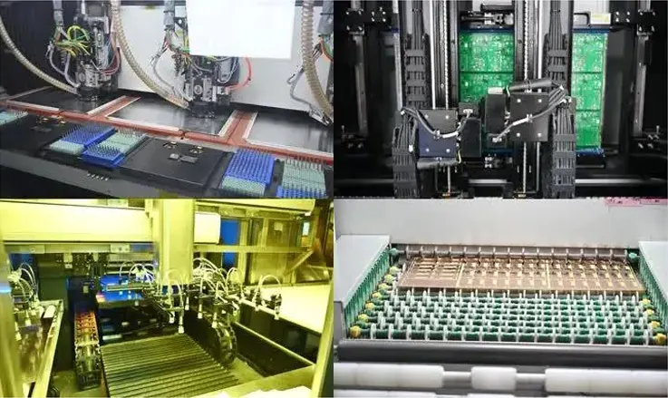
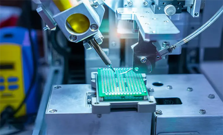
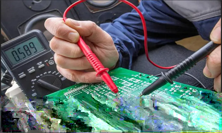
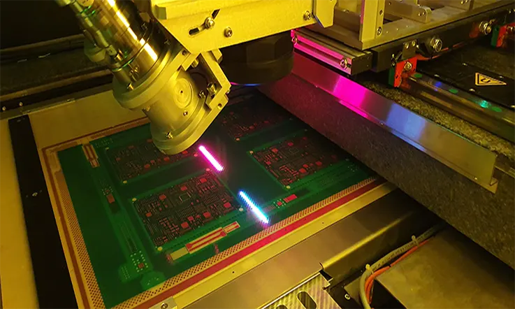
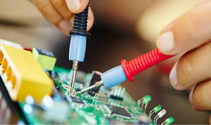
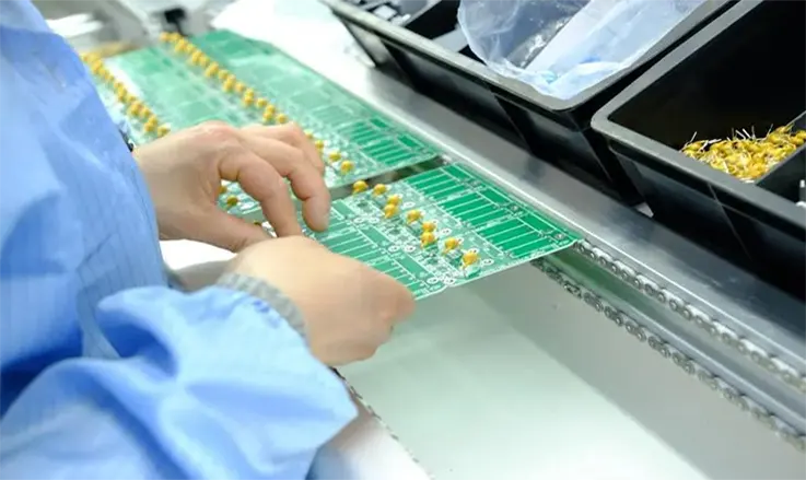
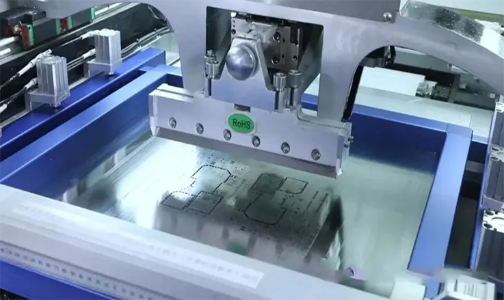
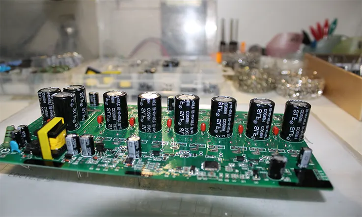
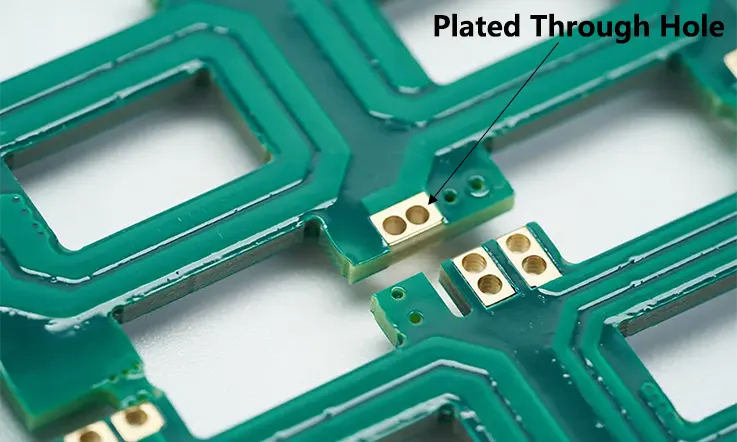
The production process for Printed Circuit Boards (PCBs) starts with the design phase, handled by an electronics engineer. Following this, PCB manufacturers produce the board as per the design specifications, after which an assembler inserts the electronic components onto the board. A quality control testing process is the final step in ensuring that the end product meets the required standards.
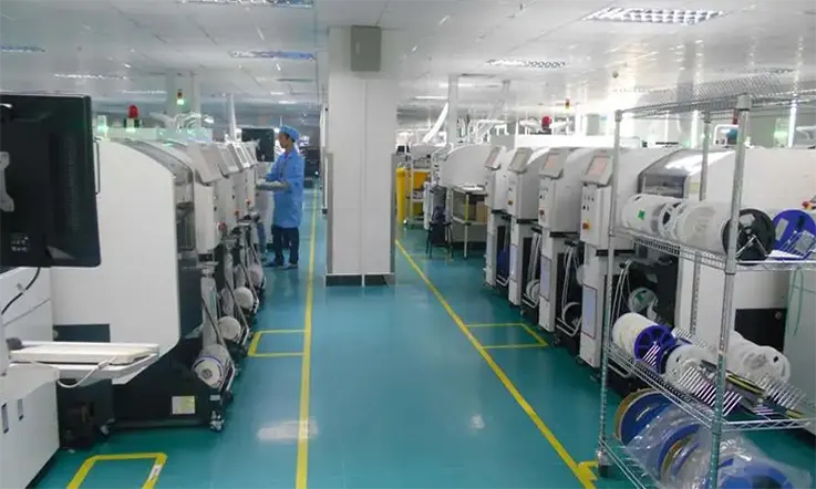
PCB manufacturers differ in the range of services they offer. While some firms provide a comprehensive range of services, others specialize in only one or two areas of the PCB production process. In such cases, clients may have to collaborate with multiple manufacturers to obtain the desired end product.
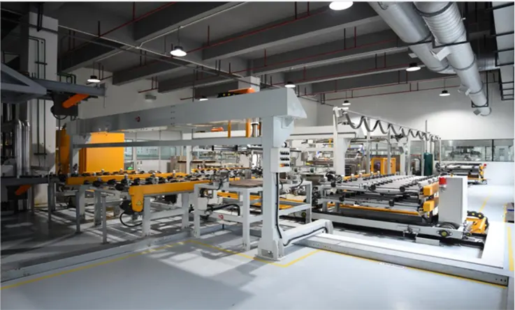
As an industry, PCB manufacturing comprises many small private enterprises that offer their own PCB manufacturing services, while larger electronics companies have incorporated PCB departments within their organizations. In some cases, companies develop the PCB in-house while outsourcing the production and/or assembly to China, keeping such information confidential. This makes it challenging to ascertain the real size of such organizations.
What Does PCB Mean?
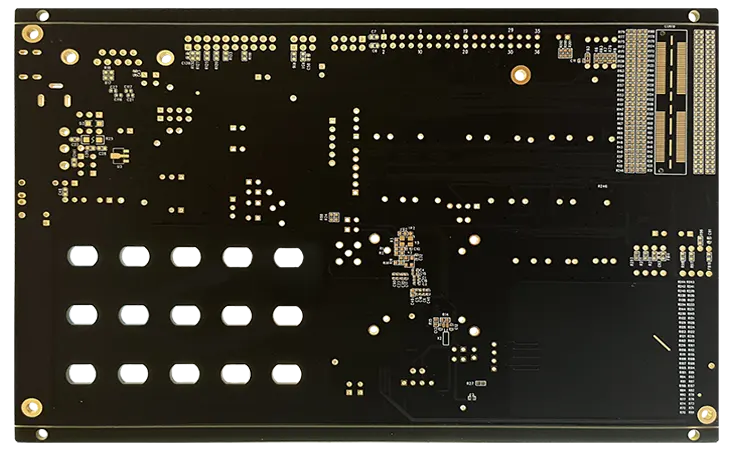
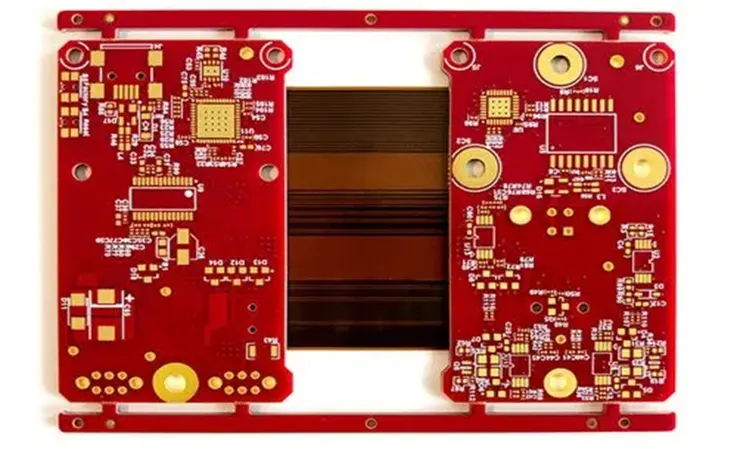
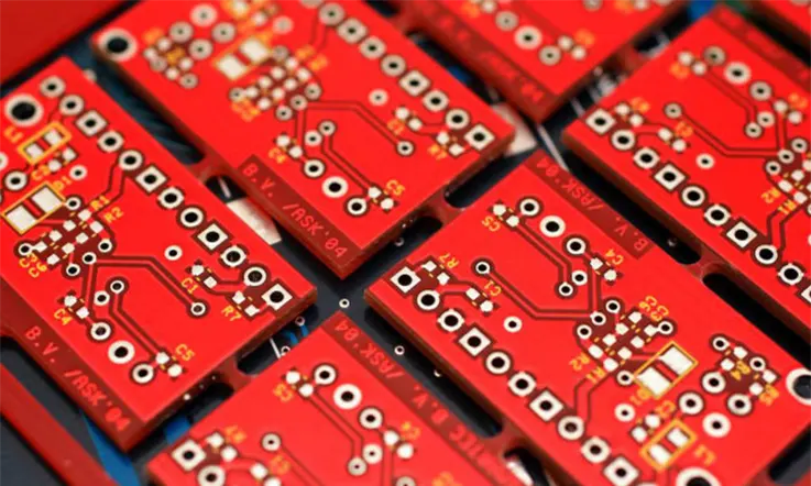
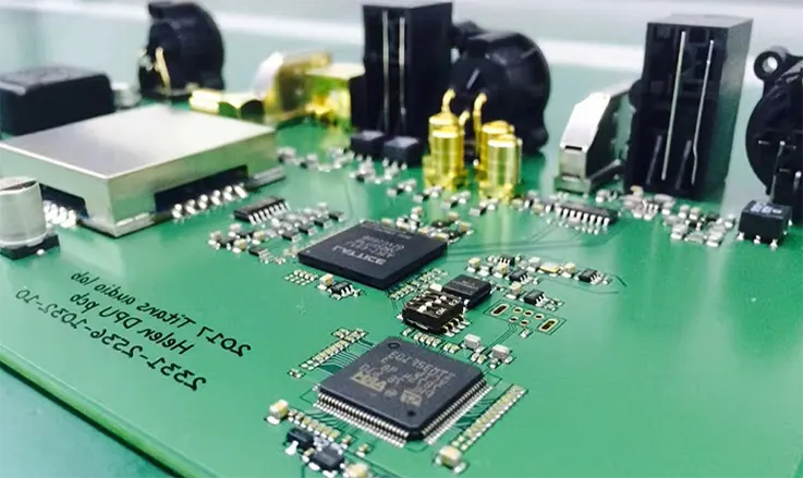
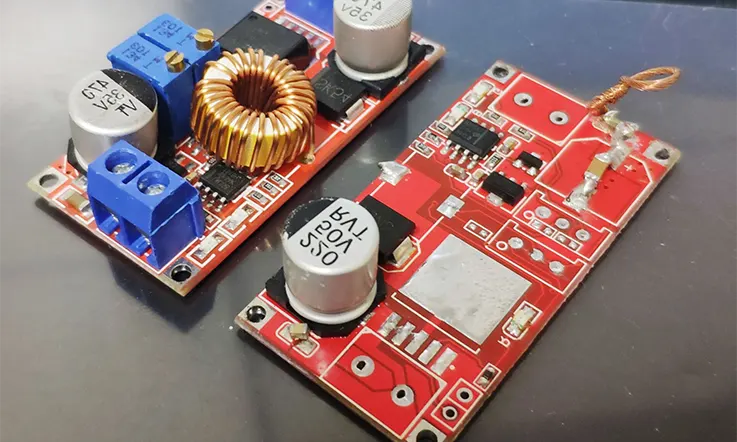
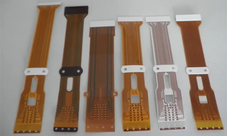
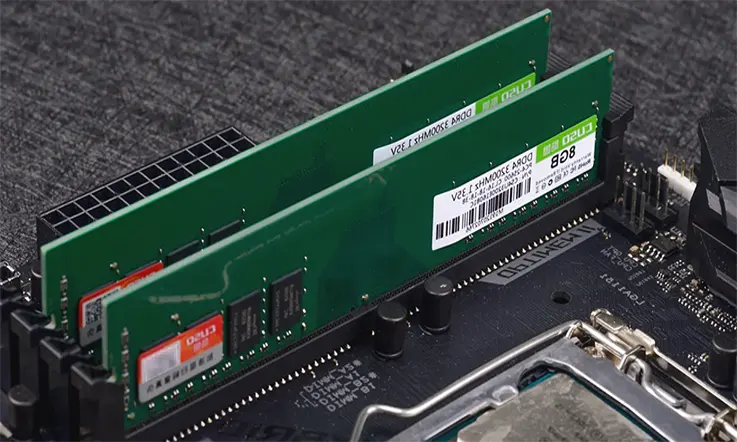
Printed Circuit Boards (PCBs) are a crucial component present in nearly all electronic products worldwide. PCB manufacturers produce various types of PCBs with varying sizes, colors, and specifications to meet the specific needs of different applications. PCBs can be rigid, flexible, or a mix of both, also known as rigid-flex boards.
Manufacturing PCBs involves significant investments in infrastructure, a large workforce, technical expertise, and favorable industrial conditions due to its time-consuming and costly nature. In recent years, the PCB sector has shifted to industrial zones in Taiwan, Mainland China, and North America.
However, finding dependable PCB manufacturers who can deliver specialized PCB designs and production services to meet unique client requirements can be a challenging task.
It is crucial for PCB manufacturers to have the necessary expertise and infrastructure to deliver high-quality PCBs that meet the precise needs and specifications of their clients. By collaborating with reliable PCB manufacturers experienced in providing customized solutions, clients can ensure seamless production of PCBs that meet their specific applications.
Why Choose Chinese PCB Manufacturers?
There are several reasons why one might choose Chinese PCB (Printed Circuit Board) manufacturers, including:
● Cost-effectiveness: Chinese PCB manufacturers often offer lower prices due to lower labor costs and economies of scale.
● High-quality PCBs: Many Chinese manufacturers are equipped with advanced technology and equipment, allowing them to produce high-quality PCBs with precise specifications.
● Wide range of options: With China being a hub of PCB manufacturing, there are many different manufacturers to choose from, offering a range of options in terms of size, complexity, and material.
● Fast turnaround time: Chinese PCB manufacturers often have faster turnaround times due to their large production facilities and efficient supply chain networks.
● Flexibility: Chinese manufacturers can often accommodate custom orders and provide personalized services to meet the specific needs of customers.
However, it’s important to carefully research and select a reputable manufacturer to ensure the quality and reliability of the PCBs.
So Who is the Best PCB Manufacturer?
Given the critical role played by bare circuit boards in the design and production of electronic devices, it is essential to engage the services of a reliable and experienced PCB manufacturer to handle this vital task.
In the current market, the number of PCB manufacturers and companies has been on the rise, making it challenging to identify those with the requisite expertise, technology, and capabilities to deliver high-quality PCB designs.
To address these concerns, our team has conducted in-depth research to identify a select list of top-tier PCB manufacturers specialized in PCB design, manufacturing, component purchase, and assembly. Our meticulous screening process has ensured that only experienced and reputable manufacturers make the cut, allowing clients to access custom products tailored to their unique requirements
So, do you require PCB bare board manufacturing and assembly right now?
Through our 20 years of experience in the PCB manufacturing and assembly industry, we have established a sound understanding of top-performing manufacturers. Using our expertise, we present a curated list of the top 10 PCB manufacturers in China, aimed at streamlining your selection process and providing you with confidence in your choice.
1. DSBJ
DSBJ is a globally recognized technology partner that specializes in the production of crucial components for IoT intelligence. The company’s areas of expertise include Metal Precision and Telecommunication Equipment, LED PCB technologies, and Interconnect solutions.
With a strong presence in multiple countries such as mainland China, Taiwan, South Korea, India, Sweden, Germany, Poland, Estonia, Finland, the United States, and Mexico, DSBJ prides itself on fast and efficient handling of customer needs. The company offers local sales coupled with top-notch customer service and storage facilities.
DSBJ’s core products include FPC/FPCA, PCB, Rigid-Flex, Base Station Antenna, RF Filter, Technical Ceramic, Die-casting & CNC & Thermal, Sheet Metal, and Stamping.
In recent news, DSBJ has announced plans to undergo a comprehensive transformation in the lithium field. While the company’s main business was in consumer electronics, it is now committed to a transformation aimed at recreating a new DSBJ that is compatible and suitable for use in electric vehicles. The company’s extensive experience in the consumer electronics field serves as a solid foundation for this venture.
2. ZDT
Zhen Ding Tech, also known as ZDT, is a prominent Taiwanese PCB manufacturer with extensive experience of over 15 years in PCB fabrication services. The company has a robust presence across Taiwan, China, and India and specializes in large-scale PCB production and assembly services.
ZDT’s commitment to innovative research and development puts it ahead of market developments, ensuring superior levels of customer service in PCB manufacture and assembly services are achieved.
In response to the unprecedented growth and evolution of the Internet of Things (IoT) technology, Zhen Ding Tech prioritizes innovation, developing advanced technologies and high-end products that embody the future of PCBs.
ZDT is progressing with extensive research on technology solutions such as flexible PCBs, high-density interconnect (HDI), substrate-like PCBs, rigid-flex PCBs, integrated circuits, and a variety of semiconductor devices. These cutting-edge solutions have applications in various consumer products such as smartphones, wearables, laptops, smart appliances, medical, and automotive equipment.
With over 20 offices and a workforce of more than 36,000, Zhen Ding Tech offers top-notch business and technical services globally.
3. Jarnis Tech
As a PCB designer, choosing a reputable PCB manufacturer is essential to ensure successful design implementation.
JarnisTech PCB & Assembly is a prominent and respected PCB manufacturer in the industry, renowned for providing an array of exceptional services.
Unlike many other PCB manufacturers, JarnisTech PCB offers full and in-house services, starting from prototyping to complete circuit board assembly, making them an outstanding and ideal option to partner with.
Furthermore, JarnisTech PCB has developed expertise in personalized circuit board services, ensuring exceptional and customizable products for their clients’ specific project needs. As a PCB designer, you can trust JarnisTech PCB’s proficiency to deliver expertly personalized circuit board solutions.
Capabilities
As a PCB designer, performing a thorough background check on your potential PCB manufacturer before enlisting their services is a pivotal step in the design process.
When evaluating a manufacturer with whom to partner, it is crucial to assess their ability to create the specific type of circuit board required for the project.
JarnisTech is an exceptional choice for a PCB manufacturer, offering a proven track record of delivering high-quality products. With PCB design expertise of exceptional standard, JarnisTech boasts an impressive 91% success rate in meeting the PCB requirements of their customers. This exceptional capability makes them an ideal choice for your PCB design project.
Some of its PCB capabilities are as follows:
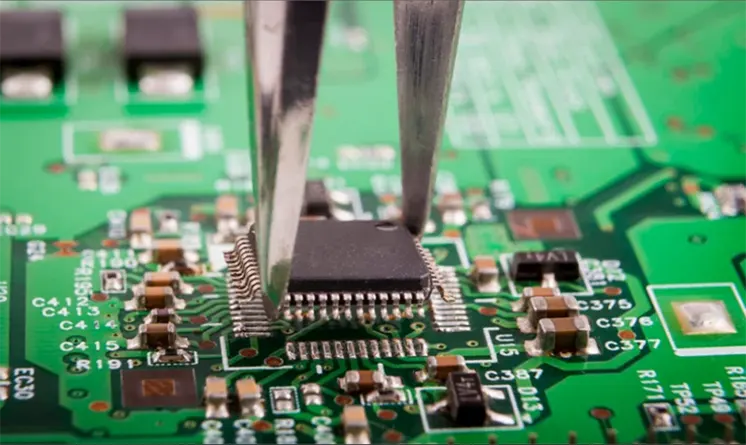
PCB Assembly
As PCB design engineers, we understand that assembling Printed Circuit Boards (PCBs) requires careful attention to detail and expertise. To simplify the process, it is beneficial to outsource your entire PCB assembly and fabrication to a renowned circuit board manufacturer that can handle the work with dedication and skill, such as JarnisTech.
JarnisTech offers both partial and full turnkey circuit board design services to cater to your specific project requirements. With partial turnkey PCB design services, you can provide some of the circuit board components, while JarnisTech handles the rest, including sourcing necessary parts and building the circuit board.
Furthermore, JarnisTech provides full turnkey PCB manufacture services, handling all aspects of your Printed Circuit Board (PCB) design. As a PCB design engineer, you can rely on their expertise in the field to provide an exceptional level of service, thus giving you the freedom to focus on other project elements.
In this instance, the manufacturer will do the following:
● Acquisition of all components required for your circuit board design, ensuring that every component meets the highest quality standards.
● Design and manufacturing of Circuit boards, utilizing state-of-the-art techniques to create high-quality products that meet your specific requirements.
● Test the 2.5mil printed circuit boards and continuously verify their quality prior to final assembly.
As a distinguished PCB manufacturer, Shennan Circuits has gained recognition for providing innovative and high-quality PCBs and circuits to original equipment manufacturers (OEMs). Our company has continuously evolved over the years, adopting new trends and technologies in PCB design capabilities through extensive research.
In addition, Shennan Circuits has research and development facilities in Europe, further propelling our ability to deliver cutting-edge PCB solutions to our global clientele.
The company pride ourselves on delivering the highest quality PCB products globally, offering a complete PCB value chain spanning circuit boards, PCB testing, scheme design, and manufacturing. Shennan Circuits also offers a 3-in-1 printed circuit board design method, which includes substrate packaging, PCB design, and electronics assembly.
With over three decades of experience in PCB manufacture, design, and assembly, Shennan Circuits excels in providing rigorously tested products at every stage of production. We specialize in the manufacturing of electronic assemblies, base plates for packaging, and other electronic items, all while incorporating the latest PCB design trends.
5. Kinwong
As a PCB manufacturer, Kinwong has a proven track record of collaborating with multiple PCB consumers to provide customized solutions that meet their unique requirements.
The manufacturer attention to detail and personalized service make them an ideal partner for your circuit board design needs. We are committed to delivering efficient service and high-quality PCBs to all our customers.
At Kinwong, they specialize in producing circuit boards for various sectors, including but not limited to:
The PCB Manufacturer have extensive experience in these sectors and pride ourselves on exceeding our customers’ expectations by providing superior PCB solutions that are tailored to their specific needs.
6. Shengyi Technology
Since 1985, Shengyi Technology has been a prominent player in the PCB manufacturing industry, with its headquarters located in China.
With a strong reputation for high reliability and exceptional skill in PCB production, Shengyi Technology has grown to become an international corporation that serves customers in North America, Europe, and Asia.
The company specializes in designing and producing a range of world-class PCBs, including Rigid-flex PCBs, High-Density Interconnects (HDI), and multi-layer circuit boards. These products cater to diverse industries and technologies such as home appliances, consumer electronics, computers, and vehicles, among others.
Besides PCB manufacturing, Shengyi Technology offers a comprehensive suite of services that includes production, sales, marketing, R&D, and technical support.
7. Suntak Technology
Suntak Technology is a recognized Chinese printed circuit board manufacturer that specializes in the design, manufacturing, and selling of high-quality printed circuit boards. The company’s range of products includes high-density interconnectors (HDI), thick copper plates, integrated panels, high-frequency boards, and others, catering to industries such as industrial control, security electronics, and communication equipment.
As a distinguished PCB maker, Suntak has received numerous accolades, including the coveted 2021 Strategic Supplier Award in June 2022, for their outstanding contribution to the delivery of 5G, and the advancement of the Internet of Things. Their efforts have been duly recognized, recognizing their significant contributions to the electronics sector.
Suntak exports over 80% of its products to Europe, America, and Asia, with the objective of providing high-quality PCBs and excellent service to the electronic information sector. The company incorporates the greatest PCB fabrication processes to ensure the high quality of their products. The products undergo rigorous testing at Suntak’s facility, making them dependable for use in high-performance applications.
In addition, Suntak has implemented a comprehensive approach to PCB testing in order to safeguard the quality and reliability of its products. Each printed circuit board undergoes rigorous examination and validation prior to receiving approval for deployment. This commitment to PCB testing is a reflection of Suntak’s priority for the safety and performance of its offering
8. China Fast Print
China Fast Print is a PCB manufacturer that places a strong emphasis on technological advancement. Recognizing the potential for growth within the Printed Circuit Board (PCB) market, this company remains committed to leveraging cutting-edge and disruptive technologies for the production of world-class hardware.
With a history dating back to 1999, China Fast Print has played a significant role in the evolution of the Chinese circuit board industry. Through the establishment of two manufacturing campuses located in Yixing and Guangzhou, this company has demonstrated its commitment to delivering innovative solutions that meet the evolving needs of its customers.
A key value held by China Fast Print is its unwavering focus on meeting the circuit board requirements of its clients. Through collaboration with over 4,000 manufacturing, R&D, and service firms across the globe, this company has established a reputation for providing a unique and reliable circuit board manufacturing process.
As a result of its collaborations with over 4,000 manufacturing, R&D, and service firms, China Fast Print has made significant contributions to the development of robust circuit boards utilized across a diverse range of industries. These sectors include rail transit, semiconductors, industrial control, medical electronics, telecommunications, automotive electronics, computers, and peripherals.
Having initially established its presence in the China PCB market, China Fast Print has since expanded its offerings to more than 100 countries across the globe. Currently, the manufacturer operates over 30 customer service centers across various regions, including China, the United Kingdom, and the United States of America.
9. Hannstar Board
HannStar Board, previously known as Pacific Technology Industrial Co., Ltd, was acquired by Walsin Lihwa in 1998. Formerly a subsidiary of Anda Pacific Technology Corporation (Liechtenstein), the company officially launched for trading on the OTC market in February of 2001 and was later listed on the TWSE on August 25, 2003.
The core business of HannStar Board is the manufacturing and sale of printed circuit boards (PCBs). The company produces 2 to 26-layer PCBs for an array of electronic applications, including servers, network communications equipment, laptop computers, flat-screen TVs, game consoles, set-top boxes, industrial computers, and enterprise electronics. In order to ensure high-quality outputs, the company employs the use of cutting-edge machines and equipment, primarily sourced from Europe, Japan, Taiwan, Israel, and the United States.
The company’s flagship products include double-sided PCBs, multi-layer PCBs, SLC multi-layer PCBs, thick copper PCBs, and high-density interconnect PCBs. HannStar Board is committed to providing top-of-the-line solutions utilizing the most advanced manufacturing technology available.
10. Wus Printed Circuit (Kunshan)
WUS Printed Circuit Co., LTD is a China-based PCB manufacturer that was founded in 1972 under the name WUS, offering a comprehensive suite of PCB manufacturing, distribution, and after-sales services. Their products specialize in an array of electronic applications, including consumer electronics, vehicle boards, industrial equipment, communication boards, motherboards, mobile phones, digital cameras, notebooks, and other digital devices, amongst others. WUS Printed Circuit Co. LTD has established itself as a reputable PCB supplier worldwide, providing its products to both domestic and international markets.
Factors to Consider When Choosing PCB Manufacturers
When choosing a PCB manufacturer, certain factors should be considered. The manufacturer should be capable of manufacturing boards that meet your specifications.
● Quality and Certifications: Quality is a critical factor to keep in mind at all times. Choose a manufacturer that places a high priority on quality during circuit board production. Additionally, consider the manufacturer’s quality management system. ISO certification is mandatory for a PCB manufacturer. This certification indicates that the manufacturer has implemented a comprehensive quality management system.
Production yield percentage and test yields should also be considered. The manufacturer should provide this information for review. Other certifications, such as A-600, IPC J-STD, and A-610, may also be available.
● Expertise: Expertise is another critical consideration when selecting a PCB manufacturer. Expertise refers to the combination of knowledge and skills necessary for PCB fabrication. There are numerous PCB manufacturers with extensive experience in the production of high-quality PCBs. Inquiring about the manufacturer’s capabilities can be particularly helpful.
● Technology and equipment: The manufacturer’s technology and equipment can have a significant impact on the quality and performance of your PCBs. Look for a manufacturer with up-to-date, advanced equipment.
● Cost: The cost of the manufacturer is another factor to consider since there can be variations in pricing among different PCB makers. Some PCB fabricators have premium prices, but the cost of a circuit board is determined by a number of factors, including material costs, the number of layers, and the type of PCB assembly technology used.
● Timely Delivery: Meeting deadlines is another critical consideration when selecting a PCB manufacturer. It is essential to deliver on time. The manufacturer’s track record should be checked, and they must be able to deliver within the specified timeframe.
● Customer service: Look for a manufacturer that provides good communication, responsive customer service, and support throughout the PCB production process.
● Location: Consider the manufacturer’s location and proximity to your business. A local manufacturer may offer faster shipping times and easier communication, but a manufacturer further away may offer better prices or specialized expertise.
Final Thoughts
JarnisTech Offers Unbeatable PCB Services
In the ever-expanding PCB market, an increasing number of electronic PCB manufacturers and printed circuit suppliers are emerging. However, it is essential to identify a partner with the necessary expertise and equipment to deliver the high-quality PCB design you require.
Choosing an appropriate Printed Circuit Board Manufacturer may demand a significant amount of time and effort, but JarnisTech simplifies the process by offering an extensive range of PCB solutions at your fingertips.
As a dedicated multilayer circuit board manufacturer, JarnisTech is committed to gaining your trust and becoming your preferred partner for all your PCB requirements. We continuously invest in our manufacturing area and workforce to remain adaptable and innovative in adopting new PCB trends while ensuring the highest level of customer satisfaction.
Whether you require PCB prototyping, small PCB production, or mass PCB production, JarnisTech has the capabilities and expertise to meet all your PCB design needs. Take advantage of our unparalleled customer service by requesting a PCB quote today.
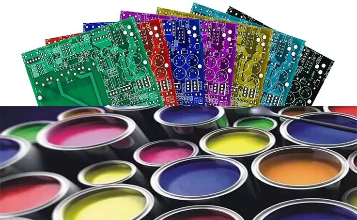
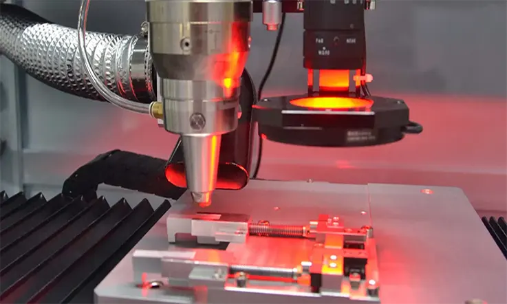
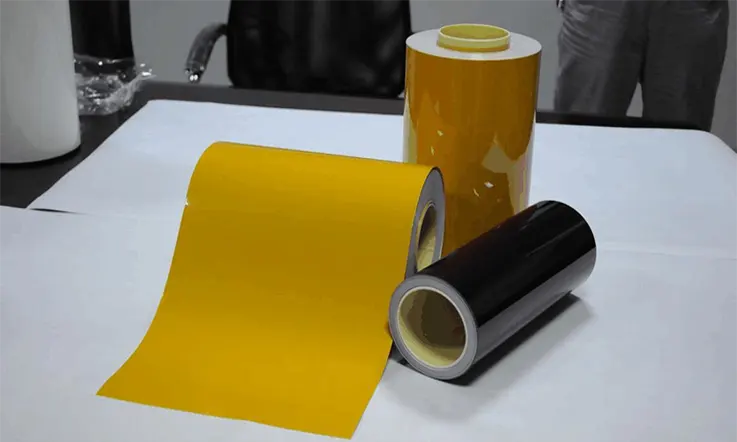
Carbon ink is a type of ink that contains conductive carbon particles, typically in the form of carbon black, mixed with a binder material. The carbon black particles are small and form a dense and continuous network, making the ink electrically conductive.
When applied to a non-conductive substrate such as paper, plastic, or even a PCB substrate, the carbon ink creates a conductive pathway or trace. The ink adheres to the substrate and dries, forming a solid and consistent line of conductive material.
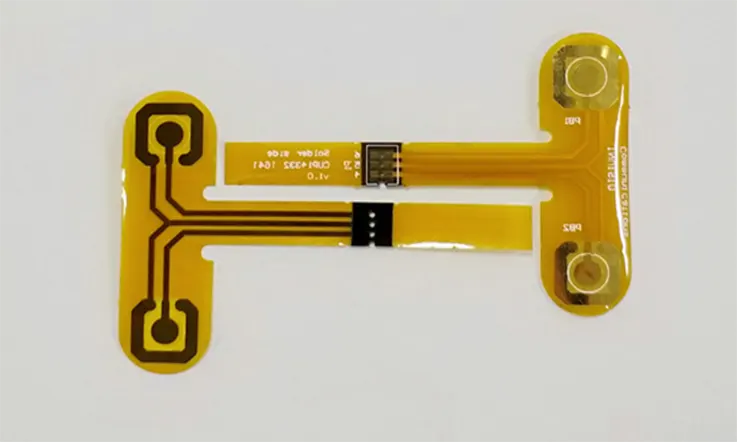
In the case of PCBs, the carbon ink is printed onto the substrate using various printing methods such as screen printing or inkjet printing. The carbon ink traces replace the traditionally used copper traces on the PCB, forming the electrical connections between components. Carbon ink is useful for creating flexible circuits, as it can be applied to a variety of substrates, allowing for more design flexibility while maintaining electrical conductivity.
What Is Conductive Carbon Ink?
Conductive carbon ink is a type of ink that contains carbon particles dispersed in a conductive polymer matrix or solvent. It is used in various applications, including printed circuit board fabrication, membrane switches, sensors, and other electronic components. When applied, the ink can create conductive traces, electrodes, and circuits on the surface of a substrate, enabling the flow of electrical current.
Carbon ink is preferred over traditional metals in certain applications due to its flexibility, low cost, and ease of application. It is also resistant to corrosion and can withstand extreme temperatures, making it suitable for use in harsh environments.
What Is Conductive Carbon Ink PCB ?
Conductive Carbon Ink PCB, also known as CCI PCB, is a type of printed circuit board that utilizes carbon inks to create conductive traces and pathways. These carbon inks are typically made of a mixture of carbon particles and a binding agent and can be printed onto a non-conductive substrate to form the circuits.
As we know, Carbon ink, a thermally setting conductive carbon paste, is frequently utilized in the assembly of printed circuit boards (PCBs). This ink can be printed via silkscreen methods on a PCB board, connecting neighboring copper features to create a conductor between traces or between traces and components. The cured carbon ink layer transforms into a thick protective film with some resistance which is commonly referred to as Carbon Thick Film PCB or Printed Carbon Resistors (PCR).
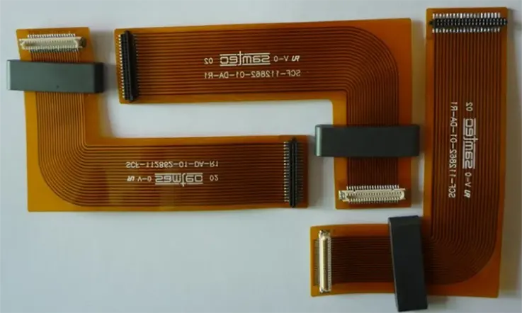
The term “carbon paste” may also be utilized to refer to conductive carbon ink, and it can be employed for printing on a wide variety of base materials including FR-4, PTFE, metal cores, and polyimide, which are utilized in rigid PCBs, flex circuits, and rigid-flex boards.
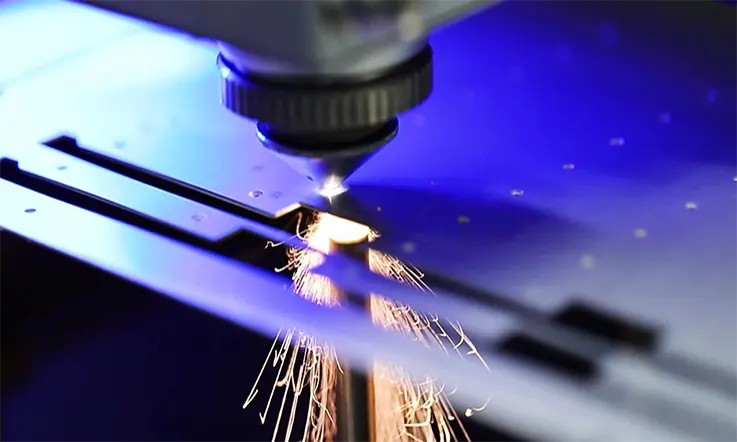
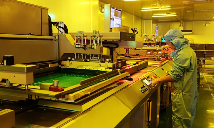
Printing Process of Carbon Ink PCB
● Resistance tolerance control.
The manufacturing process for conductive carbon ink PCBs is similar to that of silver ink PCBs, but there are some differences to note. During operation, gloves must be worn for safety purposes. It is necessary to adjust screen-printing speed and ink suction pressure to achieve optimal printing results, requiring careful testing. The screen stencil, scraper, and carbon oil must meet the specific requirements outlined by the MI engineer.
● Prior to use, it is essential to ensure that the carbon ink is thoroughly mixed and its viscosity falls within an acceptable range, as determined by a viscometer. After use, the container must be promptly sealed to prevent ink drying out.
● In preparation for printing, all PCB boards require removal of plate grease, oxide, and other pollutants. The quality assurance team inspects the carbon plate before official production commences to verify quality.
● Drying temperature for carbon PCB is set to 150 degrees Celsius for 45 minutes, while carbon ink holes require 150 degrees Celsius for twenty minutes. After the product has been removed from the oven, quality assurance must conduct an adhesion test and assess the carbon resistance.
● Each carbon ink screen version is good for a maximum of 2,500 printing times. Afterward, it must be returned to the network room to be re-dried in preparation for the subsequent version.
Important Elements for Producing High-quality Carbon Ink PCB
Producing high-quality carbon ink PCBs requires a combination of several important elements. These elements involve materials, equipment, processes, and personnel. Here are some key factors that contribute to the production of high-quality carbon ink PCBs:
● High-quality Materials: It is essential to use high-quality materials such as carbon ink, copper-clad substrates, and other essential components to ensure excellent performance and durability. The carbon ink should have a consistent viscosity, conductivity, and adhesion properties to guarantee optimal results.
● State-of-the-art Equipment: Best-in-class equipment throughout the production line is necessary to achieve precise control of printing, curing, and other manufacturing processes. This includes screen printers, lasers, ovens, and other specialized equipment.
● Rigorous Quality Control: A rigorous quality control system is critical in ensuring that each and every aspect of the manufacturing process adheres to the highest standards. This could include monitoring the viscosity and other properties of the carbon ink, verifying the integrity of PCB substrates, and ensuring that the printed lines and ink thickness adhere to specific tolerances.
● Skilled Personnel: A team of skilled personnel is essential for operating and maintaining the equipment in a professional manner. This incudes skilled technicians, quality control personnel, and engineers who work together to ensure that the manufacturing process adheres to the highest standards.
By leveraging these key elements, manufacturers can produce high-quality carbon ink PCBs that have excellent performance, consistency, and reliability.
Advantage of Carbon Conductive Ink PCB
Carbon conductive ink PCB offers several advantages over traditional PCB manufacturing methods:
● Flexibility: Carbon conductive ink is more flexible than metals and can adapt to curves and other shapes, making it a better choice for PCBs with unusual geometries or flexible substrates.
● Low Cost: Manufacturing costs for carbon conductive ink PCBs are lower than those for traditional metal-based PCBs because carbon ink is less expensive and requires less production time and processing time.
● Resistance to Corrosion: Carbon conductive ink is resistant to corrosion, making it suitable for use in harsh environments.
● Ease of Application: Carbon conductive ink can be easily applied to PCBs using screen printing techniques or other methods, making it a simpler process than traditional metal-based PCB manufacturing.
● Environmental Friendliness: Carbon conductive ink is environmentally friendly as it is composed of mainly carbon and is free from toxic metals such as lead or cadmium.
● Precision: Carbon conductive ink is superior in achieving very fine pitch circuit design and interconnections, as carbon ink can be printed consistently thinner than metal-based PCBs.
So, carbon conductive ink is a desirable option for manufacturers aiming to produce efficient, cost-effective, and reliable PCBs.
Disadvantage of Carbon Conductive Ink PCB
While carbon conductive ink PCBs offer many advantages, there is also a potential disadvantage to keep in mind:
● Limited Conductivity: The conductivity of carbon conductive ink can be lower than that of copper or other metals, which may impact the performance of PCBs that rely on high levels of conductivity.
● Less Solderability: Carbon conductive ink may not be as solderable as metals due to its lower melting point, which could create challenges when installing electronic components in PCBs.
● Lifespan: Carbon conductive ink PCBs may have a shorter lifespan than metal-based alternatives when faced with high voltage or high temperature environments.
● Heat Dissipation: Carbon conductive ink is not as efficient in heat dissipation as copper, which could impact the ability of the PCB to withstand high temperatures.
● Lack of Compatibility: Carbon conductive ink may not be compatible with all substrates, so special care must be taken to ensure that the substrate material used is suitable for the application.
when considering the use of carbon conductive ink PCBs, it is important to weigh these potential disadvantages against the perceived benefits to ensure that it is the best solution for the intended application.
Applications of Conductive Carbon Ink PCBs
Conductive carbon ink PCBs have a wide range of applications, including:
● Consumer electronics: Carbon ink PCBs can be used in products such as mobile phones, tablets, and laptops to replace traditional copper-based PCBs. They are particularly useful for flexible circuits that require bending or folding.
● Medical devices: Conductive carbon ink PCBs are used in a variety of medical devices, such as pacemakers, hearing aids, and medical sensors. They can be used to create medical devices that are flexible and conform to the body, improving patient comfort.
● Automotive industry: Conductive carbon ink PCBs are used in automotive applications, such as sensors, lighting, and displays. They are particularly useful in the design of electric and hybrid vehicles where lightweight and flexible circuits are required.
● Aerospace and defense: Conductive carbon ink PCBs are widely used in aerospace and defense applications such as satellites, weapon systems, and communication systems. The lightweight and flexible nature of carbon ink PCBs makes them ideal for use in space and military environments.
● Green energy: Carbon ink PCBs are also used in green energy applications, such as solar panels and wind turbines. They are used to create circuits that are conductive, lightweight, and flexible, making them ideal for use in energy harvesting and storage systems.
Comparison of Conductive Carbon Ink PCBs With Other Types of PCBs
Here are some key differences and similarities between conductive carbon ink PCBs and other types of PCBs:
● Material: Conductive carbon ink PCBs use carbon ink traces instead of traditional copper traces. This makes them more flexible and lightweight than copper-based PCBs.
● Cost: Carbon ink PCBs are generally less expensive than copper-based PCBs, especially for small production runs.
● Performance: Carbon ink PCBs offer comparable performance to copper-based PCBs in terms of electrical conductivity, thermal stability, and resistance to environmental factors such as humidity, temperature, and UV radiation.
● Manufacturing: Carbon ink PCB production is a simpler and more eco-friendly process compared to traditional copper-based PCBs. It requires less energy and resources to manufacture, reducing waste and environmental impact.
● Design: Carbon ink PCBs allow for more design flexibility due to their ability to be printed on a range of substrates, including flexible and non-flat surfaces. Copper-based PCBs, on the other hand, are limited to rigid and flat substrates.
In summary, conductive carbon ink PCBs offer a cost-effective and flexible alternative to traditional copper-based PCBs, with similar performance characteristics. Their unique material properties make them ideal for a range of applications requiring lightweight and conformable circuits.
Future Developments in Conductive Carbon Ink PCB Technology
The future development of conductive carbon ink PCB technology is likely to involve the following areas:
● Higher performance carbon inks: The development of carbon inks with higher conductivity and lower resistance will lead to improved performance and reliability of carbon ink PCBs. This will increase their application in electronic devices with higher power requirements.
● Integration with emerging technologies: Carbon ink PCBs have already found application in printed and flexible electronics. Future developments will likely involve integrating carbon ink PCBs with emerging technologies such as wearables, internet of things, and 5G networks.
● Manufacturing technologies: Developing more efficient and eco-friendly production processes will lower the cost of manufacturing carbon ink PCBs and reduce their environmental impact. Advances in inkjet printing and roll-to-roll printing will likely play a significant role in this area.
● Application-specific improvements: Carbon ink PCBs can be optimized for specific applications by modifying the ink or substrate properties. This will enable performance enhancements in areas such as thermal management, EMI shielding, and high-speed signal routing.
● Sustainability: Carbon ink PCBs are already an eco-friendlier alternative to copper-based PCBs. Future developments will likely focus on making the production and disposal of carbon ink PCBs even more sustainable, with an emphasis on reducing waste, recycling, and using renewable materials.
The future of conductive carbon ink PCB technology is promising, with ongoing advancements expected to expand their range of applications and make them a more competitive alternative to traditional copper-based PCBs.
Summary
JarnisTech is a renowned provider of high-quality services at cost-effective prices for customers seeking printed circuit board (PCB) fabrication and assembly solutions. Our company is a one-stop-Factory, offering a comprehensive range of services that cater to the diverse needs and requirements of our customers. Our product offerings also include a wide selection of conductive carbon ink and other types of ink that are suitable for use in PCB projects.
Our team comprises of highly skilled employees with over 20 years of combined experience in the PCB industry, making them among the market’s best. We also provide bespoke product customization services tailored to individual customer needs. Our team of dedicated quality assurance specialists guarantees compliance with international quality standards.
We take pride in providing extensive information and support to our customers, with trained personnel available around the clock to attend to our clients’ product queries and other concerns. No order is too small or large, as we are equipped to produce PCB boards in any number, including single units. Our products can be delivered worldwide, thanks to our global distribution network. Customers can easily place purchases or make inquiries by accessing our contact page.
At JarnisTech, our commitment to quality, customer satisfaction, and service reliability remains unparalleled in the industry.
As a PCB designer, it is important to acknowledge that the manufacturing of IoT devices necessitates a specialized breed of circuit boards that pose unique design and manufacturing challenges. Unlike conventional electronic products, IoT devices push the boundaries of manufacturers and designs. Manufacturers have been facing difficulties keeping up with the rapid-scale adoption of new technologies in the market, further complicating the manufacturing processes involved.
The design and integration of IoT components into circuit boards require strict adherence to design rules and complex component integration, with the additional challenge of constantly evolving technology. Manufacturers must continually adapt to new technological advancements to remain competitive, which can prove to be a significant challenge. This has led to the slow adoption of IoT technology by companies and organizations, with more than half of them finding it challenging to implement.
However, despite these challenges, the production and sale of IoT devices continue to increase substantially due to market demands. As a PCB designer, it is imperative to understand the effects of IoT on PCB manufacturing to ensure the successful implementation of IoT projects.
What Is IoT ?
The emergence of the Internet of Things (IoT) marks a convergence between the physical and digital domains, where devices other than personal computers can connect to IP networks. While smartphones represent the most prominent examples of IoT, recent advancements, such as the proliferation of apps for running household appliances and utilities, the advent of wearable technology, and vehicles equipped with data accessibility, underscore the boundless potential of IoT.
Despite consumer electronics being the first to come to mind when thinking of IoT, industries such as manufacturing, transportation, and healthcare surpass personal electronics and automobiles in leveraging the transformative potential of the IoT revolution. Therefore, these large-scale industries require PCB designs that are innovative, confer flexibility, and deliver high-speed connectivity to enable globally optimized operations.
Advantages of (Internet of Things) IoT
●Enhanced Connectivity: IoT provides seamless and smart connectivity between devices, enabling the exchange of real-time data, and improving operational efficiency.
●Improved Efficiency: IoT streamlines processes, automates tasks, and optimizes resource utilization for enhanced productivity and reduced costs.
●Greater Insights: IoT-generated data offers new insights into complex systems and user behaviors, allowing for better decision-making, improved user experience, and new opportunities for innovation.
●Enhanced Safety and Security: IoT devices can enhance safety measures by monitoring and identifying potential hazards while also maintaining security through secure encryption protocols.
●Increased Revenue: IoT improves product performance, service delivery, customer engagement, and support services, all of which contribute to increased revenue.
●Cost Reduction: IoT can provide significant cost reductions in areas such as energy consumption, inventory management, maintenance, and supply chain optimization.
So, we can think that IoT offers a broad range of advantages, ushering in opportunities for innovation, automation, and enhanced productivity across various industries.
Disadvantages of (Internet of Things) IoT
While the Internet of Things (IoT) brings many benefits, it also presents certain challenges and disadvantages, which include:
●Security Risk: IoT devices can be vulnerable to cyber-attacks, and as a result, data privacy and security can become major concerns.
●Complexity: IoT devices can be complex and require specialized skills in design, development, and implementation. This can result in higher development costs, reduced interoperability, and integration challenges.
●Interoperability: The lack of standardization in IoT devices and platforms can make interoperability difficult, limiting their effectiveness and creating fragmentation in the market.
●Accessibility and Reliability: IoT devices rely heavily on connectivity and network accessibility, which can be limited or disrupted by various factors such as geographic location, network issues, or power outages.
●Data Overload and Management: With the abundance of data generated by IoT devices, weakness in data collection, analysis, and processing of large sets of data can become a challenge, overwhelming systems and impacting efficiency.
●Ethical Issues: IoT raises several ethical concerns such as far-reaching data collection capabilities, privacy, and security threats, and the potential bias and responsibility associated with automated decision-making.
Therefore, while IoT offers numerous benefits, measures are required to address the challenges that arise in its implementation, safeguard data privacy, address reliability issues, and standardize processes to allow for proper operation and integration.
What Is PCB in IoT ?
The Internet of Things (IoT) refers to a network of various electronic devices that are specifically designed to communicate with each other through internet connectivity, employing software, sensors, and other technologies in their creation. An example of IoT in action is the connection of a smartphone to a refrigerator to utilize a smartphone app that enables users to examine its contents remotely. Using this technology, individuals can remotely monitor their homes by connecting their phones to CCTV cameras and even shop for needed items while away from home, while still keeping track of their refrigerator’s contents.
IoT Printed Circuit Boards (PCBs) provide power to IoT hardware, serving as the foundation or fundamental structure upon which these devices are built. Given the congestion of RF bandwidth by high-frequency IoT applications, unwanted meddling and safety issues may arise. Accordingly, PCB designers must shield all sensitive electronics to reduce hazards from EMI, while an efficient grounding mechanism provides protection against interference issues. In summary, IoT PCB design is essential for safety and health reasons
PCB Design Requirements for the Internet of Things
The emergence of IoT technology has brought about unprecedented challenges in PCB design engineering. Designers are now required to consider issues that were not previously encountered, such as evaluating consumer interaction with everyday items that have been equipped with IoT functionality. This represents a shift in focus from how users interact with electronic devices to assessing how they engage with traditionally non-tech items. Consequently, the PCB design process is changing, with an increased emphasis on reliability and minimal assembly errors. This is particularly crucial given the steadily growing demand for household products equipped with IoT features. PCB design engineers must strive to meet these challenges by incorporating high-quality standards into their work and continually adapting to new trends in the IoT.
The Changes in the IoT PCB Design Process
The process of developing IoT-optimized products involves a series of critical phases, beginning with an evaluation of potential new form factors, followed by the selection of appropriate PCB materials and layouts. Throughout the product design flow, it is essential to consider the requirements for assembly into a completed product.
One of the most significant impacts of IoT is the blurring of the lines between mechanical and electronic aspects, as well as between the product itself and its PCB form. Collaboration between PCB designers, mechanical designers, and electrical engineers throughout the entire design process has become increasingly relevant, representing a departure from previous assembly line-like procedures. As such, teamwork and cross-functional communication have become essential elements in creating successful IoT products. By working collaboratively, the team can ensure that the PCB design is seamlessly integrated with the mechanical and electronic aspects, resulting in a high-quality, functional product that meets the needs of consumers.
IoT PCB Design Tips and Recommendations
When it comes to designing a PCB for optimal IoT performance, several key design areas require special attention. As a PCB design engineer, it is crucial to keep these elements in mind and implement strategies that ensure a flawless design. Below are some critical design areas and tips for enhancing the quality of your IoT PCB design:
●Wireless Connectivity: Incorporating internet connectivity into an Internet of Things (IoT) printed circuit board (PCB) is pivotal to its functionality. Consequently, selecting suitable wireless modules and RF circuit components is paramount in the data collection and transmission process. As a PCB design engineer, it’s essential to bear in mind power consumption, network range and speeds, as well as security requirements when determining the most appropriate components for your design.
●Power Consumption: IoT devices must consume minimal power to ensure long battery life and optimal performance. Utilize low-power components, and consider implementing power-saving features such as sleep modes to minimize power consumption.
●Connectivity: Strong and reliable data connection is a critical aspect of IoT devices. Ensure that your PCB design includes antenna components with adequate range and bandwidth. Proper placement of wireless modules can also enhance signal strength.
●EMI/RFI: Electromagnetic interference (EMI) and radio-frequency interference (RFI) can compromise IoT device performance. Proper grounding, power management, and isolation techniques can prevent EMI and RFI and ensure the device operates reliably.
●Sensor Integration: IoT devices rely on sensors to collect and transmit data. Ensure that you have selected the appropriate sensors for your device, and that they are correctly placed, secured, and interlinked.
●Form Factor: IoT devices come in various forms, including wearables, home appliances, and industrial equipment. Ensure that your PCB design is optimized for the specific form factor, taking into account factors such as size, weight, and interface.
●Product Fitting: In PCB design, it’s crucial to consider not only the physical size of the board but also ensuring the shape of the design can be seamlessly integrated into the intended IoT form. Due to the non-traditional materials commonly used in IoT products, such as mesh or plastic components, circuit layout often needs to adapt to ensure optimal functionality. Effective virtual prototyping is essential to verify that the design can effectively accommodate any necessary modifications to meet the product’s requirements.
●Reliability Standards: As technology continues to evolve, so do the standards for ensuring the trustworthiness of electronic devices. In the case of flexible circuit boards, designers must adhere to specific guidelines to prevent their boards from cracking under varying stresses and environmental changes, thus ensuring their reliability. Consumers expect electronic devices to operate accurately and reliably for extended periods. Therefore, designers are under significant pressure to create products that can withstand a range of potential conditions. To achieve this, many designers turn to simulation software to test their designs thoroughly.
By taking into account these important design areas, you can strengthen your IoT PCB design and create high-performance, reliable IoT devices that are sure to meet the demands of today’s tech-savvy world.
Challenges of Integrating IoT devices in PCB Design
Integrating IoT devices in PCB design can present several challenges, including:
Power management: IoT devices typically operate on limited power sources, such as batteries. PCB designers must carefully manage power consumption to ensure that IoT devices can operate efficiently without draining their power sources too quickly.
Size and space constraints: IoT devices are often smaller than traditional components, requiring PCB designers to incorporate miniature components that can be challenging to work with. This also poses challenges when it comes to layout and routing of the components, especially when dealing with high-density designs.
Connectivity protocols: IoT devices use a variety of connectivity protocols, including Wi-Fi, Bluetooth, Zigbee, and cellular networks. PCB designers must ensure that their designs are compatible with the chosen protocol and that they can handle the specific requirements of each protocol.
Security: IoT devices pose significant security risks, and PCB designers must incorporate robust security features into their designs to ensure data privacy and prevent hacking and other cyber threats.
Testing: IoT devices and sensors can be complex, and testing them can be challenging. PCB designers must ensure that their designs can be adequately tested to verify that they meet performance requirements and can integrate seamlessly into the larger system.
PCB Design Considerations for Manufacturing IoT Devices
The design of a PCB for IoT devices requires a comprehensive strategy that takes into account several critical considerations, such as security, interoperability, power/processing capabilities, scalability, availability, controllability, and the operational environments. IoT devices can be deployed in various settings, including consumer, industrial, or enterprise environments. To ensure the smooth and efficient manufacture of IoT devices, PCB design engineers must determine the specific device type and classification and address any design considerations and Design for Manufacturability (DFM) concerns accordingly. This requires close collaboration with Contract Manufacturers (CMs). Below is a list of essential PCB design considerations and DFM concerns categorized by IoT device type and classification.
Device Class (Devices)
PCB Design Considerations
DFM Concerns
Consumer(home appliances, wearables, smart TVs)
Board flexibilityboard size, EMI, signal integrity, high density interconnect (HDI)
Component placement, trace lengths, stackup, via types, connector constraints, bend radii
Industrial(pumps, motors, ID tags)
Board strength, thermal capacity, high voltage, integration with mechanical design
Board material, trace sizes, thermal reliefs
Enterprise(computing equipment, security systems, temperature control)
Power reliability, connectivity, RF, high frequencies, module connectivity
While it’s critical to prioritize the key PCB design considerations mentioned earlier, it’s important not to overlook other factors that could impact the DFM. PCB design engineers must ensure that their DFM takes into account the capabilities and manufacturing equipment of their Contract Manufacturers (CMs). This ensures that the PCB design meets the essential requirements of manufacturing IoT devices effectively. Adequate attention to both fundamental and nuanced design considerations allows the successful creation of IoT devices that meet the necessary standards for reliable and effective performance.
IoT in relation to PCB design and manufacturing
The advent of IoT has significantly impacted PCB design and manufacturing as it necessitates the integration of wireless communication capabilities into numerous smart objects flooding the market. The incorporation of RF technology components into a product imposes stringent design rules on the entire system, including the Printed Circuit Board, and mandates the execution of specific testing and validation processes at the end of the manufacturing process.
The addition of one or more chips dedicated to wireless connectivity for diverse applications, including industrial sensors, wearable devices, and location trackers, presents significant design challenges for the product design team. As such, PCB design engineers must be proficient in addressing these challenges, including selecting appropriate components, adhering to design rules, and effectively integrating wireless capabilities into products, to produce reliable and sustainable IoT devices.
●Integration:PCB design engineers face significant challenges when integrating wireless communication capabilities into the compact form factor of IoT devices. This requires the careful selection and placement of additional components, making efficient use of available space within the device.
●RF Design:Designing a product with embedded RF communication capabilities necessitates the adherence to stringent design rules aimed at optimizing the radio performance while minimizing interference with other components and systems. Moreover, it is crucial to comply with relevant regulations and standards concerning RF pollution, power transmission, and other related issues. PCB design engineers should demonstrate proficiency in RF design techniques to ensure that IoT devices operate effectively and efficiently without interfering with other systems or breaching regulatory provisions.
This impacts the PCB routing as well:
When designing RF circuits, it is crucial for PCB design engineers to consider impedance matching during signal routing. The absence of impedance matching leads to substantial power losses, as well as hazardous signal reflections along the PCB traces. As many systems and RF modules have a standard impedance of 50 Ω, it is advisable for RF PCB traces to have an identical characteristic impedance. Microstrips and striplines are two frequently used trace types on PCBs, with the latter particularly useful in 4-layer PCBs for improved routing.
Apart from stack-ups, the designer must ensure that RF signals are suitably isolated to regulate unwanted coupling with other signals. The customary method is to use a continuous ground plane situated immediately below the upper layer with components and transmission lines. The design team must also pay attention to shielding to avoid interference between the RF circuitry and the baseband section.
The PCB and product assembly processes are subject to strict requirements when designing RF circuits. Additionally, testing processes are a critical aspect that will most likely require RF testers on the line. By addressing these considerations, PCB design engineers can ensure optimal design, manufacturing, and testing of RF circuits in IoT devices.
Importance of IoT in PCB design and manufacturing
IoT (Internet of Things) has emerged as a critical technology for the world of electronics and has revolutionized PCB (Printed Circuit Board) design and manufacturing. Here are some of the key reasons for why IoT is important in PCB design and manufacturing:
●Smart Connectivity: IoT devices have sensors that allow them to connect and communicate with other devices over the internet. With IoT, PCB designers can incorporate smart connectivity features into their designs, which creates a more connected and efficient system.
●Enhanced Product Functionality: IoT technology enables PCB designers to add a wide range of functionalities to their designs. With IoT, PCBs can be designed to perform complex tasks such as monitoring environmental conditions, tracking location, and controlling other devices.
●Improved Reliability: IoT technology makes it possible for PCB manufacturers to build more reliable and robust systems. With IoT, devices can monitor and report data to help identify any potential issues before they become critical failures.
●Higher Efficiency: IoT devices and sensors can collect and analyze data, allowing for more efficient processes and optimized performance. This data can then be used by PCB designers to create more efficient systems, reducing costs and improving overall performance.
●New Market Opportunities: IoT has opened up new markets for PCB manufacturers, creating opportunities for businesses to develop new products and services that can take advantage of the connectivity and functionality of IoT devices.
Impact of IoT on PCB Industry
IoT has had a significant impact on the PCB industry, including:
●Increased demand for smart connectivity: The rise of IoT has led to an increased demand for smart connectivity in PCB designs. This has led to the development of new technologies and components that can enable this connectivity.
●Adoption of new materials: PCB designers are adopting new materials and substrates that can support the high data rates and high-frequency requirements of IoT devices.
●Greater design complexity and miniaturization: IoT devices are often smaller and more complex than traditional electronics, leading to greater design complexity and miniaturization in PCBs.
●New testing and validation requirements: IoT devices require more stringent testing and validation, including testing for wireless connectivity and power efficiency.
●Increased collaboration between manufacturers and designers: IoT devices require close collaboration between manufacturers and designers to ensure the seamless integration of hardware and software components.
Therefore, IoT has led to new innovations and opportunities in the PCB industry, leading to higher performance, increased connectivity, and improved user experiences.
The Future of PCB Design for the IoT
●The fast-growing IoT industry has raised questions regarding whether PCB design for IoT will become increasingly individualized or standardized. Despite every IoT device having unique characteristics, there are common requirements that suggest a growing trend towards mixing and matching the same design protocols repeatedly.
●IoT presents immense opportunities and challenges for the PCB industry, and its growth is expected to continue. This trend has the potential to blur the lines between electrical and mechanical engineering, leading to the development of even smaller, high-performing minicomputers. The demand for IoT devices is predicted to grow exponentially, and this could pave the way towards a future filled with innovative technological solutions.
●As the electronic industry steers its way through this evolving landscape, it aims to develop PCB designs that can cater to the complex needs of IoT while handling the predicted increases in demand. The establishment of standardized design protocols can further simplify the manufacturing process, resulting in IoT devices that are reliable, efficient, and maximize their performance capabilities.
Summary
The advent of the Internet of Things (IoT) has brought about a profound transformation in the electronics sector, revolutionizing PCB design and manufacturing as a pivotal technology. Its significance lies in its ability to facilitate intelligent connectivity, enhance product functionality, elevate reliability and efficiency, while simultaneously opening up fresh market avenues. As IoT progresses, its influence on PCB design and manufacturing will inevitably grow, leading to the development of more innovative and efficient products that are better adapted to the constantly evolving technology landscape. It is evident that IoT and PCB design and manufacturing are intimately related and will continue to drive the future of the electronics industry.
As an electronic manufacturer, you may have encountered inquiries regarding the relevance of a 94v0 circuit board. This type of circuit board is sometimes compared to conventional PCBs, leading to questions about its advantages. These uncertainties usually arise from a lack of understanding of the 94v0 circuit board.
In demanding environments with fluctuating temperatures, engineers require a durable and reliable device that can endure prolonged use. As a result, circuit engineers have developed methods for evaluating and selecting suitable materials for PCB replication. With mounting interest in this area, it becomes essential to establish a framework for evaluating and testing different PCB design materials. This article offers a well-researched explanation of the 94v0 circuit board, shedding light on what it entails and its relevance to the electronic manufacturing industry.
What Is FR4 94v0?
FR4 94v0 is a type of circuit board material that has been tested and classified with a flame retardant rating of UL 94v0. The FR4 refers to the grade of the woven glass-reinforced epoxy resin that makes up the substrate, and the 94v0 rating indicates that the material meets certain fire safety standards, such as the ability to self-extinguish within 10 seconds after being exposed to a flame. This type of circuit board material is commonly used in various electronic applications, such as consumer electronics, industrial control equipment, and automotive electronics, where fire safety is an important consideratio
What Is a FR4 94v0 Circuit Board?
As engineer designers, it is vital to recognize the 94V-0 circuit board as a type of printed circuit board intended to provide highly dependable performance across diverse applications. This premium quality, reliable PCB is frequently utilized in many different electrical goods, and is generally made from conductive material, primarily copper, with insulation.
The 94V-0 rating is a UL flame resistance rating allocated to specific types of PCBs. This certification confirms that the board has been thoroughly tested and verified to be flame resistant up to 94 volts. As far as safety is concerned, this rating is of the utmost importance. This rating denotes that the 94V-0 circuit board can be safely employed in a range of environments, including those with high humidity and temperatures. Engineer designers must keep the 94V-0 rating in mind when selecting circuit board materials to guarantee that the circuit boards employed in their designs meet the prescribed safety standards
Classifications of FR4 94v0 Circuit Board
As a PCB manufacturer, it is essential to understand the UL 94 flammability test, which is a procedure that evaluates the flame resistance of material. The test requires using a specimen made from plastic, measuring 127 × 12.7 mm (5 x 0.5 in.) in size and meeting the minimum acceptable material thickness criteria.
To conduct the test, the specimen is exposed to a flame, and the resulting reaction is categorized according to six classifications by UL, each denoting varying degrees of flame resistance. PCB manufacturers must have an in-depth understanding of the UL 94 flammability test to ensure that the materials used in the manufacturing process meet the accepted standards for flame resistance, ultimately ensuring the safety and reliability of their products.
● V-0:The V-0 test is the most stringent test for PCBs in terms of flammability, conducted on a vertical scale with a burn time that should not exceed 10 seconds. This test does not allow any flammable drips to ensure safety.
● V-1: Similarly, the V-1 test is also conducted on a vertical scale, and the specimen must stop burning within 30 seconds without emitting any drips.
● V-2: The V-2 test is another vertical flame test, offering a 60-second burn time and allowing for minor flame dripping.
● 5VA: In the case of the 5VA test, the surface burning ends after 60 seconds, and the specimen should not ignite for more than 60 seconds even after five applications of the test flame. Neither the specimen nor the surface should have a burn-through hole, with the optimal specimen thickness for 5VA material being 2.5 mm.
● 5VB: With the 5VB test, the surface fire should be extinguished within approximately 60 seconds, and flame drips are not permitted under the test conditions. However, the specimen may suffer from burn-through or have holes forming on its surface.
● HB: Finally, the Horizontal Burn (HB) fire rating is the lowest of the UL 94 flammability criteria, requiring that a specimen with a thickness of 3 to 13 mm has a burn rate of less than 40 mm per minute. Moreover, the fire must extinguish before it reaches 100 mm of the test sample’s length.
A thorough understanding of the UL 94 classification system is necessary for PCB manufacturers to ensure the safety and reliability of their products.
Benefic of 94V-0 PCBs
As a reputable PCB manufacturer, we understand the technical aspects and unique advantages of using circuit board 94V-0 for various applications. The material used in the construction of this board has achieved a high rating in the UL 94V-0 flammability test, signifying that it is flame retardant, which is essential in ensuring safe operation in many electronic devices.
● Incorporating standardized connector pins into the design of the 94V-0 board simplifies component mounting and soldering during the assembly process. This streamlined design optimizes manufacturing efficiency and enables quicker turnaround times.
● The multi-layer structure of the 94V-0 circuit board is a recent advancement in PCB design that enhances assembly density by utilizing conductive copper lining and insulating materials. This innovative design allows for large circuit formations on small boards, ultimately reducing the board’s size and overall manufacturing costs.
● Another notable benefit of using 94V-0 rated circuit boards is their superior signal integrity capabilities. These high-quality boards prevent electromagnetic interference (EMI), ensuring a reliable signal transmission for improved device performance.
In a word, the excellent performance of the circuit board 94V-0 can be attributed to its flame retardant material, standardized connector pins, high assembly density, and signal integrity capabilities. As a PCB manufacturer, we highly recommend this board for electronic applications that require optimal performance and reliability.
How does the Electronics Industry Define 94v0 Circuit Boards
In the electronic industry, it is essential to have a clear understanding of the construction and functionalities of circuit board 94V-0. This high-quality PCB consists of a layer of conductive material, mainly copper, which is overlaid with insulation. The insulation restricts the flow of current and provides protection against potential damage. The board also contains an array of soldered components such as resistors, capacitors, and transistors, which are integral to building a functional circuit.
The circuit board 94V-0 has undergone stringent quality checks to ensure resilience to harsh weather conditions, making it resistant to moisture, temperature fluctuations, and shock. In addition, the board has been designed to withstand high voltages, up to 94 volts, permitting its use in a wide range of applications.
The circuit board 94V-0 surpasses several industrial standards and regulations, including being UL-listed and RoHS-compliant, indicating that it meets the essential requirements set for Restriction of Hazardous Substances. This board is also compliant with the European Union’s Low Voltage Directive.
In summary, circuit board 94V-0 presents an excellent alternative for electronic industry seeking a dependable, high-quality PCB. The board is engineered to deliver dependable performance, endure harsh environments, and comply with industrial regulations. Additionally, with its UL listing and RoHS-approved status, the board is suitable for an extensive range of applications, and its flame-resistant rating of up to 94 volts renders it appropriate for any application.
JarnisTech-the Best Manufacturer of 94v-0 Circuit Board
As a distinguished PCB manufacturer, JarnisTech has an impressive track record of over 20 years in producing, assembling, and testing printed circuit boards. We offer a broad range of services, including manufacturing UL 94V-0 rated PCBs and other types of PCBs. At JarnisTech, we prioritize delivering high-quality products, ensuring timely delivery, and providing exceptional customer service every step of the way.
Furthermore, we offer component procurement services through the Bill of Materials (BOM) and Surface Mount Technology (SMT) processes. Additionally, our Through-Hole Technology (THT) assembly method for circuit boards comes with rigorous testing to ensure the delivery of a PCB free of defects.
For a swift quotation on your UL 94V-0-rated printed circuit board, kindly click on this link to receive an immediate quote. Do not hesitate to contact us here for any queries or clarifications regarding our services. At JarnisTech, we ensure that our clients receive the best PCB manufacturing, assembly, and testing solutions for their electronics business needs.
How to Manufacture FR4 94v0 boards?
The process of manufacturing FR4 94v0 circuit boards typically involves the following steps:
● Preparing the base material: The manufacturing process starts with cutting a standard-sized FR4 sheet into smaller sizes. The sheets are then cleaned, and sometimes pre-baked to remove any moisture.
● Applying a copper layer: The cleaned and pre-baked FR4 sheet is then coated with a layer of copper using various techniques such as electroplating or lamination.
● Printing the circuit design: The next step involves printing the circuit design onto the copper layer using a process called photoengraving. This involves covering the copper layer with a photosensitive layer, curing the layer with UV radiation, and then exposing it to a light source to transfer the circuit design.
● Etching the circuit: Once the circuit design is printed, the sheet is etched with a chemical solution to remove the unwanted copper material, leaving only the desired circuit pattern.
● Drilling the necessary holes: The sheet is then drilled with small holes at specific locations (where components will be attached) using a high-speed drill or a laser.
● Applying soldermask and silkscreen layers: The board is then coated with a soldermask layer to protect the copper traces from oxidation and ensure that the solder adheres only to the desired areas. A silkscreen layer may also be applied to label the components and add logos or other information.
● Surface finish: The final step involves applying a surface finish to protect the board from environmental factors and improve its electrical conductivity. Common surface finishes include HASL (Hot Air Solder Leveling), ENIG (Electroless Nickel Immersion Gold), and OSP (Organic Solderability Preservative).
After completing these manufacturing steps, the board is carefully inspected for defects and tested to ensure that it meets the required specifications before it is used in electronic device.
Advantages and Disadvantages of Using FR4 94v0 Boards
Advantages of Using FR4 94v0 Boards
● High level of thermal stability and low thermal expansion.
● Good electrical insulation properties and dielectric constant.
● Excellent mechanical strength, rigidity, and dimensional stability.
● Economical compared to other high-performance materials.
● Relatively easy to work with and can be fabricated using standard PCB manufacturing processes.
● High resistance to moisture, chemicals, and environmental factors.
● Good flame resistance properties.
Disadvantages of Using FR4 94v0 Boards
● Not suitable for high-frequency applications due to high losses.
● Relatively low thermal conductivity compared to metals and ceramics.
● May not be suitable for applications requiring high power handling capacity.
● Can be difficult to drill accurately due to its high hardness.
● Not suitable for applications that require low dielectric loss or stability in humid environments.
It’s worth noting that specific advantages and disadvantages may vary depending on the particular application, and careful consideration of the material’s properties is essential to ensure it’s the right choice for the application.
Applications of FR4 94v0 Circuit Board
It is crucial to recognize the diverse applications of circuit board 94V-0 in various industries. This high-quality board is widely utilized in consumer electronics, industrial machinery, aerospace, and medical equipment. Its versatility and reliability make it a popular choice in these industries.
Circuit board 94V-0 can be used to construct intricate circuits while also providing dependable performance in different operational environments. The board’s flame retardant material and high assembly density make it a suitable option for applications that demand high performance.
In addition, circuit board 94V-0’s broad range of use cases across various industries underscores its exceptional quality and design. As PCB design engineers, it is essential to consider the potential advantages of using 94V-0 rated circuit boards when selecting a PCB for specific applications.
What are the Most Compatible PCB Substrates with 94V-0?
In the realm of printed circuit boards (PCBs), the substrate is a vital component that is utilized to separate the two copper layers. It is responsible for providing the necessary support to the entire structure of the bare PCB. PCB substrates can be made of a single material, such as ceramic, or a composite material, which is a combination of multiple materials to create a premium-quality substance with excellent physical, chemical, mechanical, and environmental characteristics. Materials like FR-4 and Ceramic are two such examples of PCB substrates that are highly suitable for meeting the UL 94V-0 test requirements. These materials possess exceptional fire-resistant properties and are ideal for use in electronic applications where safety is of utmost importance.
● FR-4: FR-4 is a composite material composed of fiberglass, either woven or non-woven, that is impregnated with an epoxy resin. This particular substrate material is the most widely used in the realm of printed circuit boards (PCBs). Moreover, FR-4 is a fire-retardant material, which means that it has the ability to resist the spread of fire.
● Ceramic: Ceramics serve as another exemplar of a fire-resistant substance that has inherent properties which prevent ignition. Additionally, ceramics possess several notable attributes, such as strong mechanical strength, a smaller loss tangent, and a higher dielectric constant that remains stable. However, the drawback of ceramics is their susceptibility to crack when exposed to elevated temperatures.
Comparison of FR4 94v0 with Other Circuit Board Materials
● Cost: FR4 94v0 circuit boards are relatively inexpensive compared to some high-performance materials that can be more expensive.
● Thermal Conductivity: FR4 94v0 circuit boards have relatively low thermal conductivity, which can limit their heat management capabilities. Materials with high thermal conductivity, such as metal and ceramic, offer better thermal management.
● Dielectric Constant: FR4 94v0 circuit boards have a dielectric constant of 4.4, which is similar to commonly used materials such as polyimide (PI) and polytetrafluoroethylene (PTFE), but lower than materials such as polyimide film and zirconia.
● Moisture Absorption: FR4 94v0 circuit boards have a relatively high moisture absorption rate, which makes them susceptible to environmental humidity and other factors.
● Mechanical Strength: FR4 94v0 circuit boards have good mechanical strength and rigidity, but they are more brittle compared to metal materials.
● Flame resistance: FR4 94v0 circuit boards are classified with a flame retardant rating of UL 94v0, which prevents the flame from spreading during a fire. Other materials may have different flame retardant ratings.
● Manufacturing Difficulty and Ease of Use: FR4 94v0 materials are relatively easy to manufacture and use, and they can also be efficiently machined into other materials. The manufacturing and machining processes for other high-end materials can be more complicated.
● Resistance to Chemicals and Environmental Factors: FR4 94v0 circuit boards have high corrosion and chemical resistance and environmental stability but cannot withstand extreme environmental and chemical exposure.
● Electrical Conductivity and Reliability: FR4 94v0 circuit boards offer good electrical performance and high reliability. Some high-performance materials offer better electrical characteristics and reliability but typically require higher handling and usage demands.
● Availability and Applicability to Specific Uses: FR4 94v0 circuit boards are widely used and available for a variety of applications (such as consumer electronics, military, medical, etc.). Other materials may be specific to certain applications and harder to obtain.
Note that this is a general comparison, and specific comparisons and considerations may vary depending on the application.
Why Do You Need 94V-0 Circuit Board?
This factor can be seen in three ways:
1. From the Manufacturer’s Perspective
In the realm of manufacturing, maintaining brand reputation is crucial, as producing substandard electrical equipment can lead to negative reviews and diminished sales. While cost-effectiveness may be a significant factor for certain electronic products, some high-demand applications require the use of 94V-0 printed circuit boards to achieve optimal quality. Investing in higher quality PCB boards can yield several benefits, such as enhanced brand recognition, greater ratings, increased credibility, and improved profitability. Manufacturers might consider raising product pricing to reflect the added value of superior hardware.
Alternatively, manufacturers may choose to implement a grading system, wherein devices featuring 94V-0 circuit boards receive a higher grade compared to those with conventional PCBs. This enables customers to choose whether they prioritize price or quality factors. Adopting this flexible pricing model permits manufacturers to charge competitive prices for low-quality gadgets, while premium pricing may be assigned to high-quality items.
2. From the Perspective of an Electronic Developer
For independent electronics developers, building long-lasting electrical equipment can boost their chances of securing new project opportunities and recommendations, similar to manufacturers. Integrating high-quality electrical circuit boards in one’s project is one effective method to achieve exceptional product performance and surpass customers’ expectations.
In academic settings, electrical engineering students must demonstrate proficiency by crafting dependable electrical circuits in their school projects to attain high grades. The devices should be capable of withstanding adverse conditions and endure rigorous testing without any failure to showcase the students’ engineering abilities.
3. From the Consumer’s Perspective
As a discerning customer, you face the decision of either purchasing low-priced electrical equipment at the cost of compromising quality or investing in high-quality equipment that may entail higher costs but promises longevity.
Unbranded electronic equipment is typically fitted with low-grade PCB circuit boards that may lack fire retardant properties. Conversely, branded and genuine grade products are more likely to feature advanced circuit boards that have been tested to withstand intense heat. This approach not only ensures safety but also provides an enhanced level of functionality and reliability.
It is worth considering that manufacturers are also striving to establish their reputation and brand image by delivering high-quality electrical products. As a result, many products in the market offer superior performance and durability.
Know More on the 94v0 Circuit Board
In the production of printed circuit boards (PCBs), the 94v0 circuit board diagram serves as a useful tool to provide a visual representation of the board’s components. These diagrams are conveniently available online, providing easy access and reference.
To ensure safety and satisfy standard device fire prevention regulations, the 94v0 PCB undergoes a series of rigorous fire tests after production.
Furthermore, the material used for a PCB, such as Fr4 94v0, is a crucial determinant that demonstrates the manufacturer’s commitment to producing high-quality boards. This selection reflects the need for PCBs that are both resilient and capable of high-performance output, highlighting the manufacturer’s dedication to delivering superior electronic products.
Summary
In summary, the 94V-0 PCB circuit board is a crucial component that offers durability and reliability, enabling electrical equipment to withstand high heat levels in even the toughest working environments. Additionally, the UL94V-0 inflammability test guarantees optimal performance and safety standards.
As a leading PCB manufacturer, we offer comprehensive PCB assembly services and are capable of creating custom 94v-0 circuit boards tailored to your project’s specific requirements.
For more details regarding our high-quality PCB design and assembly services, please feel free to contact us. We guarantee the most competitive price in the market.
In the world of technology, electronic devices and advances go hand in hand. As a result, the significance of circuit boards has gained substantial importance, making it an essential aspect that every professional in the electronic industry- including students, engineers, designers, and hobbyists- must grasp. A comprehensive understanding of printed circuit boards is crucial for professionals in the electronic industry, and this article aims to provide a detailed explanation of a vital component of PCB technology- Surface Mount Technology (SMT). By explaining the various useful aspects of SMT in the context of printed circuit boards, electronic industry professionals can upgrade their skills, and keep pace with the rapidly evolving developments in this field.
SMT: Surface Mount Technology
As PCB designers, it is essential to be aware of the technology utilized by printed circuit boards employing surface mount technology. A circuit board employing SMT may or may not have holes on their interior surface. Rather, electronic components are situated on top of copper pads and traces already present on the PCB’s surface.
Thanks to this semi-automated process, manufacturers can generate all the necessary circuit boards for their products within their own facilities. This innovative technology facilitates a straightforward attachment of electronic components to the surface of printed circuit boards in a manner distinctly different from the traditional insertion method employed by manufacturers.
SMT technology provides an alternative to the conventional approach of creating circuit boards that use through holes. Compared to the through-hole technology, SMT addresses several deficiencies and limitations due to its more contemporary iteration. In summary, it is essential for PCB designers to be familiar with SMT to effectively design cutting-edge PCBs that feature surface mount technology.
The Process of Surface Mount PCB Assembly
In the PCB industry, the assembly process for Surface Mount Technology (SMT) involves several crucial steps, with design being the most critical. Prior to beginning the design using Cadstar or Orcad, it is imperative to select the appropriate components. When necessary, alternative software design tools can be utilized. PCB designers should aim to incorporate as many design features as necessary into the PCB to enhance its functionality.
● Once the design and component selection is complete, the PCB data must be sent to the production firm, along with adherence to automation guidelines when procuring components. Crucial specifications to consider for the PCB design include surface treatment, which should be encoded into the appropriate Gerber file format before submission.
● Payment processing will trigger the delivery of package components, usually in reels. It is crucial to avoid loose components as they may require the purchase of particular feeding plates or manual placement, both of which are laborious and time-consuming.
● The next step is to print the solder paste using the appropriate supplies, including the solder paste, printing stencil, and solder paste printer. It is essential to ensure accuracy during this stage to avoid any potential errors that could lead to a disaster in subsequent phases.
● After printing the solder paste, an inspection should be carried out before proceeding to the automatic optical inspection (AOI), first article inspection (FAI), and component placement steps. Upon completion of these stages, the final assembly process is verified using x-rays to ensure that everything was assembled correctly. PCB Industry professionals should be aware of the importance of each step in the SMT assembly process to ensure high-quality end products.
Surface Mount Technology: Advantage
● Automated Assembly: For PCB manufacturers, utilizing automated pick and place equipment is a necessary aspect of the surface mount technology assembly process. This equipment facilitates the installation process of the vast number of surface-mounted components (SMT) on circuit boards, resulting in a highly efficient and precise process. High-volume components, such as passive components, are loaded automatically into the automated SMT machines from a reel. Meanwhile, other components are loaded via trays or tube feeders. This process is markedly different from the traditional plated-through-hole (PTH) components, which require manual assembly. The use of automated equipment in SMT technology enables the manufacturer to achieve high-speed, accurate and cost-efficient production, enhancing product quality and customer satisfaction, and overall profitability.
● PTH Component Commonality: In the electronic industry, surface mount technology parts have proven to be a cost-effective solution due to their smaller size and voluminous nature compared to their plated-through-hole (PTH) counterparts. As a result, SMT components frequently cost less than PTH equivalents, offering manufacturers and customers a more cost-effective solution for their electronic needs.
Moreover, there is a high demand for SMT components compared to through-hole parts, resulting in the availability of these components in the market. The supply chain for surface mount technology components is well-established, making it easier for electronic industry manufacturers to access and procure these crucial components. Overall, the electronic industry has embraced SMT technology due to its cost-effectiveness and supply-chain effectiveness, ensuring the production of high-quality electronics while achieving economic efficiency.
● Size: For designers, surface mount technology offers the benefit of producing components that are more compact than their plated-through-hole (PTH) counterparts, since long leads for insertion and soldering into holes are not necessary. This advantage allows designers to accommodate a greater number of components within a given board space, a crucial consideration when working within constrained board design environments. Such compactness afforded by SMT technology presents a significant opportunity for designers to maximize their board’s functionality while still achieving a high degree of precision and accuracy. Consequently, SMT technology enables designers to achieve greater flexibility when working with board space limitations, enabling them to produce high-quality electronic designs that fulfill their customers’ needs.
● Electrical Performance: The application of Surface Mount Technology (SMT) in printed circuit board (PCB) production has become increasingly prevalent in contemporary times. SMT PCB’s small size allows for the integration of more components while minimizing signal path length, resulting in superior signal integrity and reduced heat output compared to the Through-Hole PCB (PTH). As a result, commercial machinery manufacturers have taken to adopting SMT to fabricate a wide range of PCB devices in convenient packages. This trend fortifies the feasibility and cost-effectiveness of the technology.
Surface Mount Technology: Disadvantages
● Surface Mount Technology (SMT) is a widely used method of PCB assembly that offers improved component placement speed. However, it is not a zero-defect method and presents unique challenges during assembly.
● One of the drawbacks of SMT is that the machinery required for assembly is expensive, leading to a notable initial capital expenditure. While this cost may be offset by reducing the cost of board assembly, it may be challenging for electronic assembly manufacturers working with low-volume prototype boards.
● Additionally, SMT increases the likelihood of component misalignment compared to Through-Hole Technology (THT). This is because, with THT, the leads are inserted through the holes in the circuit board, ensuring perfect alignment of the components. However, with SMT, extra care must be taken during assembly to avoid misalignment.
SMT Manufacturing Process:7 Steps
1.Preparation and Test of the SMC and PCB
The assembly of Surface Mount Components (SMC) and Printed Circuit Boards (PCB) is a key activity that takes place in the PCB industry. During this process, great care must be taken to ensure that there are no defects. Solder pads are a vital aspect of the PCB that facilitate the proper placement of the SMC components. These pads are usually flat and made of materials such as tin-lead, silver, or gold-plated copper, and are free of perforations.
To guarantee the high quality and reliability of the final product, it is necessary to carry out rigorous testing to identify any flaws that may have arisen during SMC and PCB preparation. This testing process is essential to ensure that the components meet the required performance standards and adhere to industry best practices.
2.Stencil Preparation
During Printed Circuit Board (PCB) assembly, the process of printing solder paste onto the board is a common technique used to facilitate the placement of Surface Mount Components (SMC) accurately. To achieve accuracy, a stencil is typically used to create a fixed position for the components. The design of this stencil is based on the predetermined placement locations of the solder pads on the PCB, and is critical for ensuring that the SMC components are placed with the required precision.
The stencil’s manufacturing process typically involves creating openings at the predetermined solder pad locations to allow for the application of solder paste. This enables the accurate placement of the SMC components and ensures that the final product adheres to the required industry standards. Effectively, the quality and reliability of the PCB assembly process are directly linked to the accuracy of the stencil and its ability to create consistent component placement during the solder paste printing process.
3.Solder Paste Printing
In the field of electronic manufacturing, the process of connecting Surface Mount Components (SMC) with Printed Circuit Boards (PCB) typically involves the use of solder paste. This paste is composed of flux and tin, and is applied onto the solder pads located on the PCB using a stencil and a squeegee at an angle that typically ranges from 45 degrees to 60 degrees.
The purpose of the solder paste is to enable the formation of a strong and reliable connection between the SMC and the PCB. This connection is achieved through the process of reflow, which involves heating the solder paste to a specific temperature to enable the formation of a solid joint between the SMC and the PCB. By utilizing the stencil to apply the solder paste at a precise angle, the overall accuracy and consistency of the final product can be optimized, and any potential defects can be minimized.
4.SMC Placement
In the electronic manufacturing industry, Printed Circuit Boards (PCBs) undergo a series of processes to achieve accurate and reliable assembly. One such process is achieved through the use of pick-and-place machines. These machines are responsible for placing the PCBs on a conveyor belt, where they are then transported to the component placement area, where electronic components are attached to the PCBs.
The pick-and-place machines play a crucial role in ensuring that the SMC components are positioned precisely on the PCB, in accordance with the predetermined solder pad placements created during the stencil printing process. The accurate placement of these components is essential to ensure a reliable and efficient operation of the final product.
5.Reflow Soldering
In electronic manufacturing, reflow soldering ovens are commonly used to bond electronic components to Printed Circuit Boards (PCBs). The process involves gradually raising the temperature of the PCB and components in a series of carefully controlled stages.
● The first stage of the process takes place in the pre-heat zone of the oven. The temperature of the PCB and components is gradually and concurrently raised, with a temperature increase rate of between 1.0 and 2.0 degrees Celsius per second. This stage continues until the temperature reaches between 140 and 160 degrees Celsius.
● The next stage is the soak zone, where the boards are held at a constant temperature between 140 and 160 degrees Celsius for a duration of between sixty to ninety seconds. This stage is crucial to ensure that the temperature of the PCB and components is stabilized and that the solder paste is evenly distributed.
● The reflow zone is the next stage, where the temperature rises at a rate of 1.0 to 2.0 degrees Celsius per second, reaching a peak temperature of between 210 and 230 degrees Celsius. This temperature is required to melt the tin contained in the solder paste, bonding the component leads to the pads on the PCB. The surface tension of the molten solder assists in holding the components in their proper positions.
● Finally, the boards move through the cooling zone of the oven, which is designed to allow the solder to freeze and solidify before they leave the heating zone to prevent joint fault. This controlled cooling process is necessary to ensure that the solder bonds are stable and reliable. Overall, the reflow soldering oven is a critical part of the electronic manufacturing process for creating reliable and high-quality electronic products.
When dealing with electronic circuit boards that require double-sided assembly, it is possible to carry out a repetitive process involving the printing, placement, and reflowing of the components. This can be accomplished via the use of either solder paste or adhesive material, both of which can effectively secure the components in their designated positions. It is an industry-standard practice to apply these techniques with precision and attention to detail, ensuring that the final product meets the necessary quality standards.
6. Clean &Inspection
Upon completion of the soldering process, it is crucial to perform a thorough cleaning of the circuit boards and conduct a meticulous examination to detect any possible defects. If defects are found, rework or repair procedures are necessary before the products can be stored. Various types of equipment are commonly employed in surface mount technology (SMT), including magnifying lenses, automated optical inspection (AOI) systems, flying probe testers, X-ray machines, and other similar devices, to facilitate the inspection and evaluation of the final products.
Benefits of Using a Third-party PCB manufacturer: JarnisTech
As a electronic and electrical manufacturer, it is evident that the development of a highly automated Surface Mount Technology (SMT) construction process can offer significant fabrication advantages. However, investing in the expensive production equipment required to accomplish this task can be challenging for many businesses specializing in SMT PCB design.
Fortunately, JarnisTech provides a viable and cost-effective solution for customized PCB fabrication, leveraging our specialized resources and streamlined processes to meet our clients’ unique specifications. Our company, as one of the foremost PCB manufacturers in China, places a strong emphasis on providing exceptional customer service and reliability. With a broad range of services available, we are well-equipped to assist businesses in incorporating high-quality SMT technology into their PCB fabrication process.
Factors to Consider When Selecting Right Technology for Your Design.
The selection of appropriate technology plays a pivotal role in achieving optimal design outcomes. For instance, during the schematic design process, the component selection stage presents an ideal opportunity to decide whether to utilize surface mount technology or through hole technology. By incorporating these components early on, there is a greater chance that the PCB layout will be constructed using the right component package tracks and footprints. Nonetheless, to make informed decisions about the technology that best suits your design requirements, you need to consider the following factors:
● Rework: When it comes to the prototyping stage, do you anticipate a significant amount of circuit rework?
● Use: How will the individual components be exposed to physical contact and other forms of stress? It is important to consider the frequency of contact and whether there will be additional stresses placed on the components.
● Price:Can a cost reduction be achieved by selecting a packaging style over another? An analysis should be conducted to determine the feasibility of cost savings through the selection of a specific packaging style.
● Power:You must consider how much heat and power the component will conduct while in use.
● Availability: In the process of developing your prototype, select the package that can most easily be accessible and use the appropriate gauge.
● Performance:What type of packaging approach provides the optimal opportunity to fully realize the potential of your circuit? It is essential to determine which packaging approach will offer the greatest potential for showcasing the capabilities of your circuit.
● Assembly: Determine which package style will provide you with high-quality assembly at the lowest possible cost.
Surface-mount technology (SMT) components may potentially provide the best solution for your design needs. However, it is important to address any concerns regarding through-hole components, especially if they are required. Your PCB manufacturer can be a valuable resource in assisting you in choosing the optimum path forward. With their extensive knowledge and experience working with various component package styles relevant to printed circuit boards, they can provide valuable insights and recommendations.
At JarnisTech, we have over 20 years of experience in assembling and fabricating PCBs, and our team of professional engineers has expert knowledge of components to guide you in the right direction. They can assist with identifying part availability and associated prices. At the same time, our engineers dedicated to the PCB manufacturing process will expertly develop your board with quality based on the design criteria.
Why Used Surface Mount Technology (SMT) For PCB Assembly
It is important to recognize the benefits of the Surface Mount Technology (SMT) assembly process in modern electronics manufacturing. With SMT, a wide range of components required for modern devices can be securely fastened to the surface of the printed circuit board in increasingly smaller footprints.
SMT assembly is highly adaptable to meet specific customer requirements while also providing a highly automated solution for large volume circuit board production. For designers in need of precise and efficient assembly to meet unique specifications, surface mount technology (SMT) is often the optimal choice.
For many years, JarnisTech has been a trusted provider of surface mount PCB assembly services to customers across diverse markets. With considerable expertise in contract manufacturing, we possess a wealth of knowledge in electronic component fabrication for a wide range of industries. Our company offers end-to-end solutions such as product prototyping, testing, contract manufacturing and more, thanks to our advanced equipment and skilled personnel. For any inquiries or to obtain a price estimate, please do not hesitate to contact our office
How Might SMT Assembly Lower Production Costs?
As an electronic manufacturer, it is important to recognize the cost-saving benefits associated with Surface Mount Technology (SMT). While initial machinery costs may be a consideration, the advantages of reduced manual labor are significant and two-fold.
Firstly, SMT offers long-term cost reduction benefits by decreasing the overall cost of labor while simultaneously improving production efficiency, ultimately resulting in cost savings. The use of software to simulate the assembly process prior to actual production significantly reduces the risk of errors during manufacturing, further contributing to cost savings. In addition, SMT assembly also has the potential to eliminate delays during production, which could otherwise result in additional expenses if not avoided.
In conclusion, SMT is a cost-efficient option for electronic manufacturers, and it offers precise and efficient assembly to reduce labor costs and improve productivity, resulting in long-term cost savings.
Through-hole Vs. Surface Mount Technology
As a PCB designer, it is important to understand both the through-hole installation and surface-mount technology (SMT) processes for soldering parts onto PCB boards. Through-hole installation involves inserting component leads into drilled holes on a bare PCB and soldering them on the other side of the board. While this is a standard method, SMT offers several benefits over through-hole installation, including easier automation, faster component placement, and improved high-frequency performance.
● However, it is worth noting that SMT is not appropriate for some components, such as power semiconductors with heat sinks and large transformers. The reason for this is that SMT components are only fastened by solder on the surface of the board and are not suitable for use in severe environments.
● In scenarios where component leads travel through the board, through-hole soldering may be a better option than other methods because it allows components to withstand greater environmental stress. Through-hole technology is still preferred in military and aerospace industries, which are frequently exposed to harsh environmental conditions. Additionally, through-hole technology is helpful for test and prototype applications that require manual adjustments and replacements, as it provides easy access to internal components.
In conclusion, while SMT is advantageous in several ways, through-hole technology still has its place in certain applications. As such, PCB designers must consider the specific needs of each project and carefully weigh the benefits and drawbacks of both installation options to determine the optimal solution.
Surface Mount Technology vs. Chip Scale Packaging
Surface Mount Technology (SMT) and Chip Scale Packaging (CSP) are two different methods of mounting electronic components on a printed circuit board. Despite some similarities, such as the use of solder paste and the absence of leads, there are a few differences between SMT and CSP.
● One key difference is the size of the components used. While SMT components typically range in size from 0201 to 1206, CSP components are much smaller, with a maximum size of about 2 mm. This makes CSP ideal for miniaturized devices.
● CSP also requires a higher degree of precision during assembly, with a smaller margin of error compared to SMT. CSP component placement and soldering need to be highly accurate and precise to avoid damaging the component and ensure proper connectivity.
● Another difference between SMT and CSP lies in their reliability. CSP components can be more prone to failure than SMT components due to their smaller size and greater sensitivity to environmental factors.
SMT and CSP have their respective advantages and challenges. SMT is suitable for larger, more complex devices, whereas CSP is excellent for miniaturized electronic devices that require high-density packaging in a small space.
Components Types of Surface Mount Technology (SMT)
● Passive Components: Resistors and capacitors are regarded as staple components in the field of electronics. It is worth noting that some versions of these components are also equipped with coils that provide the necessary ability to handle high levels of electrical current. Such components are frequently utilized in electronic devices that exhibit a notable power consumption.
● Transistors and Diodes: The size of these components is very small, and they are designed to occupy a minimal amount of space. Additionally, transistors feature three legs which make them easier to handle and join through the process of soldering.
● Integrated Circuits: Integrated circuits come in a range of configurations, with varying numbers of pins. The number of pins can be as low as eight or as high as two hundred and fifty, particularly in circuits that contain microprocessors. The use of surface-mount technology (SMT) has facilitated smaller ICs without sacrificing functionality or performance, allowing for the retention of all the expected features and capabilities.
Future Trends in Surface Mount Technology
Surface Mount Technology (SMT) has undergone significant advancements over the years and is expected to continue evolving in the future. Some potential trends that may shape the future of SMT include:
● Miniaturization: With the growing demand for smaller and more powerful electronic devices, the trend towards miniaturization in SMT is likely to accelerate. SMT components are already incredibly small, but new innovations such as 3D printing and advanced materials may enable even smaller components in the future.
● Increased Integration: Another trend is towards the integration of multiple functions into a single component. This is already being seen with System-in-Package (SiP) technology, which integrates multiple components into a single module. In the future, we may see further developments that allow for even more integration of components.
● Advanced Materials: Advanced materials, such as flexible or stretchable substrates, may become more prevalent in SMT. These substrates could enable the development of devices that can bend, twist, or stretch, leading to new applications and use cases.
● Automated Inspection and Assembly: With the increasing complexity and miniaturization of SMT components, automated inspection and assembly technologies will become more critical. This may include advancements in quality control, such as AI-based inspection systems or more advanced machine learning algorithms.
● IoT and Smart Manufacturing: The future of SMT is also closely tied to the development of the Internet of Things (IoT) and smart manufacturing. These technologies will enable more efficient and automated production techniques and could lead to the creation of truly intelligent factories.
Therefore, the future of SMT is likely to be shaped by advances in miniaturization, integration, materials, automation, and smart manufacturing technologies.
To Conclude
The gradual shift from the conventional through-hole method to surface mount technology is apparent, and the latter holds a significant position in the current industry. The adoption of surface mount technology in the printed circuit board (PCB) manufacturing industry has led to a reduction in manufacturing durations for electronic goods and devices, resulting in noteworthy advancements. Consequently, the widespread incorporation of this technology is propelling the PCB manufacturing industry towards a promising future.
The Electronic Design Automation (EDA) market segment encompasses specialized software, hardware, and services geared towards supporting the complete lifecycle of semiconductor device manufacturing. This includes aiding in the definition, planning, design, implementation, verification, and final manufacturing of these devices, also referred to as “chips.”
The primary service providers in the semiconductor manufacturing space are semiconductor foundries, also known as fabs. These facilities are highly intricate and demand significant investment, and may be owned and operated by large vertically integrated semiconductor companies or independent “pure-play” manufacturing service providers. The independent model has emerged as the dominant business approach in the semiconductor manufacturing space in recent years.
What Is EDA?
EDA stands for Electronic Design Automation, which is a process of using computer and professional software tools to design, develop, analyze, verify, and produce electronic systems at the chip and circuit board levels. EDA uses automation technology to improve design efficiency and reliability, and help engineers to quickly complete the design, verification, and production of electronic products. EDA encompasses a variety of tools and techniques, including circuit simulation, layout design, timing analysis, logic synthesis, and FPGA design.
An EDA involves a group of software tools and programming systems that enhance the efficiency, accuracy, and ease of the design process for electronic systems. Beyond integrated circuits, EDA can be applied in the design of PCBs and other electronic components.
In a word, EDA is a critical tool for modern electronic design, serving as a powerful electronic computer-aided design (ECAD) resource for designers looking to create complex electronic systems using cutting-edge software tools.
How Does EDA Work?
Electronic Design Automation (EDA) is primarily a software business that enables the design and manufacture of chips through the use of sophisticated and complex software programs. These software programs function in three primary ways:
1.Simulation tools
Simulation tools that predict the behavior of proposed circuits, design tools that assemble and connect circuit elements, and verification tools that examine the logical or physical representation of the chip to check for correct connections and required performance.
2.Design Tools
Design tools are utilized to create a collection of circuit elements that implement a proposed circuit function, by both a logical and physical process. The logical process involves assembling and connecting said circuit elements while the physical process pertains to the development of interconnected geometric shapes that will construct the circuit during manufacturing. These tools are provided through a blend of fully automated and interactively guided features.
3.Verification Tools
Verification tools are essential software applications used in Electronic Design Automation (EDA) to examine the logical or physical representation of semiconductor chips to confirm that the design is connected correctly and delivers the required performance.
While EDA products are mostly software-based, in some situations, physical hardware is also used to deliver capabilities. This occurs when extremely high performance is necessary, such as during simulation and verification of large amounts of data. Dedicated hardware models of the circuit typically perform far faster than software programs that simulate the same model, making hardware delivery critical for completing various tasks within reasonable time frames (hours to days versus weeks to months). Emulation and rapid prototyping are the two main delivery mechanisms for EDA hardware.
The Development History of EDA
EDA has a history dating back to the 1950s when programmers used low-level programming languages to design digital computer systems. In the 1960s, the first tools specifically for digital circuit design appeared, such as bit-width analysis, logic synthesis, and simulation tools. In the 1970s, EDA began to enter the field of analog circuit design, including PCB and integrated circuit design.
In the 1980s, EDA became increasingly popular, and users from various fields, such as computer and communication systems, embedded systems, automotive and medical devices started to widely use it. Subsequently, EDA began to develop towards computer cloud technology, and many EDA tools were ported to cloud platforms, allowing users to use them through cloud services. Currently, EDA technology has become the core of electronic system design and has made important contributions to the development of modern high-tech industries.
The Role and Significance of EDA
EDA(Electronic Design Automation)technology forms the basis for the comprehensive development of electronic system design tools. Its significance and role include:
●Shortened development time: EDA tools accelerate the design process, reducing the time required for product development, allowing companies to bring products to market more quickly.
●Improved design efficiency: The automation features of EDA tools reduce errors, minimize repeated tasks, reduce manual workloads, and provide real-time error checking during the design process, thereby improving design efficiency.
●Improved design quality: EDA tools reduce human error and improve the accuracy of circuit routing, thereby improving the quality and reliability of the design.
●Cost reduction: EDA tools and technology can lower development costs, reduce failure rates on the production line, and lower material costs.
●Promotion of innovation: EDA tools provide numerous analysis and simulation tools, enabling designers to experiment with multiple designs and explore multiple solutions more quickly, promoting innovation in new technologies, products, and markets.
In a word, EDA technology plays a crucial role in modern electronic system design, serving as a necessary tool to enhance productivity and innovation capabilities.
Classification of EDA Software
EDA software can typically be classified into the following:
●Circuit Simulation Software: Used for analyzing and verifying circuit behavior and performance, including voltage, current, and signal transmission.
●Layout Design Software: Used for creating and editing physical layouts of PCBs, ICs, and other circuit designs.
●Logic Synthesis Software: Converts logic code in high-level hardware description languages (HDL) into circuits.
●Timing Analysis Software: Analyzes timing requirements to identify timing conflicts or optimize timing paths.
●Low Power Design Software: Used for analyzing and optimizing circuit power consumption in systems.
●FPGA Design Software: Supports the design of programmable logic devices (FPGA), including system-level design, IP cores, synthesis, layout, and routing.
●Physical Verification Software: Used for verifying physical characteristics of circuits, such as compliance of layout with specifications and signal integrity.
In addition, some EDA software implements multiple functions, such as software that integrates layout design and physical verification, as well as software that supports both FPGA and ASIC design.
Comparison of Common EDA Software
There are many common EDA software options available, and here are some of the comparisons of their features and characteristics:
●Cadence: Primarily focused on IC design, supports a variety of SIP design and test flows, including IC design, layout design, silicon validation, and system-level design.
●Mentor Graphics: Offers a variety of EDA tools, including widely-used tools in simulation, RTL synthesis, layout design, and ultimate source automatic routing (UGC).
●Synopsys: Synopsys products include integrated circuit and system-level design, silicon validation and design optimization, as well as software security and quality testing. Additionally, it also covers tools for automation, layout, and physical verification.
●Altium Designer: Provides a comprehensive one-stop solution for PCB and electronic product design, supporting the entire process from prototype design to production manufacturing.
●Proteus: Mainly used for simulation and circuit design of modular electronic circuits, with the characteristic of being easy to use.
●KiCAD: It is a highly recommended EDA tool for PCB design and circuit simulation, boasting several advantageous features. As open-source software, it is available for free, including the code, and offers a comprehensive range of capabilities typically found in proprietary tools. One example is its 3D viewer, which enables interactive canvas inspection of PCB board layouts, along with a Gerber file generator, artworks, an extensive library, and a bill-of-materials generation system. Another substantial benefit of KiCAD is that there are no limitations in terms of size or layers.
●Autodesk Eaglerepresents an inexpensive option in PCB design software that is tailor-made for beginners. The acronym stands for “Easily Applicable Graphical Layout Editor.” With Fusion 360 software from Autodesk, the tool provides additional electrical and mechanical features to enable a detailed analysis and verification of designs. Eagle has a multi-window GUI with several automation features that simplify the design process, including auto-routing, task scripting, design check, electrical rule checking, and more.
●Pulsonix, a product by UK-based company WestDev, is an advanced PCB design tool exclusively available for the Windows platform. Its intuitive interface and diverse range of capabilities are particularly noteworthy. Among its advanced PCB design features are flexi-rigid design, chip-on-board, embeddable components on PCB layers, definable snapping tolerance for accurate component placement, advanced selection mask browser, and dynamic copper pour to automatically repair damaged copper areas.
●EasyEDA is a web-based PCB design platform that eliminates the need for offline setup or installation. The online platform offers a complete range of capabilities that can be found in paid PCB design tools. These capabilities include instant schematic capture from various file formats, layout design, circuit routing, auto-routing, library creation and management, and cloud-based team collaboration and project management tools.
●DipTrace PCB Designer is a software solution intended primarily for those who need to create schematic diagrams and PCB layouts. The application consists of four sub-modules, namely the Schematic Capture Editor, Component Editor, Pattern Editor, and PCB Layout Editor.
●SolidWorks PCB is a highly productive tool that efficiently combines ECAD (electronic computer-aided design) and MCAD (mechanical computer-aided design) for seamless integration of electro-mechanical components with PCB layout. The software’s advanced capabilities enable designers to work with electronic, mechanical, and embedded software designs in a single environment, thereby optimizing the design process and reducing time to market.
It is necessary to choose the appropriate EDA tool according to specific needs or projects. These tools have their unique functions, suitable for different circuit design and development tasks, and can significantly improve the efficiency and quality of electronic product development.
EDA Tool Tips That Will Make You a Successful PCB Designer
Conducting thorough research on EDA tool vendors and selecting a vendor with a track record of success is a worthwhile practice. This may allow for efficient initiation of work processes with the provision of dependable tools. To clarify doubts or inquiries, one should not hesitate to contact the support line or participate in user groups. These available resources can aid in understanding the tools thoroughly, thus optimizing system performance.
Numerous EDA tool vendors are available; however, Cadence is a reputable and established option. With extensive experience in providing the highest level of technology in PCB design systems, Cadence has a comprehensive understanding of the requisites of PCB designers such as yourself. Their high-level OrCAD PCB Designer features diverse and advanced design tools that are essential in producing optimal results.
Applications of EDA
(Electronic Design Automation) technology is widely used in the design, validation, and production of various circuit boards and chips, as well as the development and testing of electronic systems and devices. Here are some applications of EDA:
●Integrated Circuit Design (IC Design): Designing and manufacturing integrated circuits, including digital and analog ICs, microprocessors, memories, and microcontrollers.
●Internet of Things (IoT): Developing and designing embedded systems, embedded sensor IoT nodes, embedded wireless communications, IoT cloud services, etc.
●Automotive electronics: Designing vehicle electronic systems, including vehicle electrical, control systems, in-vehicle entertainment, and autonomous driving, etc.
●Communication systems: Designing and developing communication system components, including wireless gateways, modems, digital signal processing, and optical transmission components.
●Medical devices: Designing and developing various medical devices, including medical image and signal recognition systems, medical electronic therapy devices, electroencephalography (EEG), electrocardiography (ECG), and X-rays, etc.
In short, EDA technology plays an important role in the design, manufacturing, and testing of modern electronic systems and devices, and supports the development of numerous application areas with its advanced functions and performance.
Roles of EDA in IC design
In chip design, EDA plays an instrumental role in mitigating risks and minimizing costs associated with trial and error. Since most chip products cannot be altered after manufacturing, and their designs are both complex and costly, EDA serves at least three fundamental purposes in the design process.
●Firstly, EDA tools are capable of converting complicated physical problems into quantitative models, simulate circuit processes in virtual software, and replicate various effects during chip development, thereby allowing designers to quickly identify potential design defects and mitigate risks.
●Secondly, EDA tools enable designers to simulate and analyze optimal solutions for various performance, power consumption, cost, and other conditions while ensuring proper logic functionality. Solving multi-objective constraint problems is critical for designing chips that meet various operational requirements and reducing trial and error costs.
●Thirdly, EDA tools enable the verification of model consistency, ensuring that the logic functions of the chip remain consistent throughout multiple design stages. Overall, EDA serves as a fundamental underpinning in chip design, enabling rapid identification and resolution of design risks while promoting optimal chip performance, lower costs, and higher design efficiency.
Therefore, Why EDA is so Important In Integrated Circuit design and Manufacturing?
Semiconductor chips have evolved to become incredibly intricate structures that are composed of a vast number of circuit elements, and interactions between these elements can be subtle or complex. Furthermore, the manufacturing process variations can result in even more complicated interactions and behavioral changes. Without sophisticated automation, managing this level of complexity would be nearly impossible. EDA tools are essential to address this issue by providing advanced technology that manages the entire chip design and manufacturing process, enabling efficient design workflows and addressing the inherent complexity of chip development.
It should also be emphasized that errors in a manufactured chip can be catastrophic, leading to an entire project’s failure. Unlike software, which can be updated or patched, chips are permanent, and any error in design or manufacturing will have permanent consequences. Therefore, it is essential to design and manufacture chips with the utmost accuracy and precision, which can only be achieved through the use of EDA tools.
Overall, EDA technology plays a vital role in the modern chip industry, enabling efficient management of chip complexity and eliminating the cost, time, and resource drain incurred by frequent errors and shortcomings that inevitably arise in the absence of automation. By providing powerful EDA capability, design accuracy and reliability are optimized, and a company’s risk profile is minimized, ensuring business success and maximizing customer satisfaction.
Final Words
EDA tools serve as the backbone of the integrated circuit design and manufacturing process, as well as the vehicle for integrated circuit design methodologies. They act as the linkage and bridge between the design and manufacturing phases. To complete the design process and manufacture integrated circuits, PCB Layout designers need to leverage EDA tools. Given the escalating complexity of chip design, integrated circuits leveraging advanced process nodes can host billions of semiconductor devices. As the design complexity scales up, chip design without utilizing EDA is no longer feasible.
Now, the domain of chip design has shifted to cover system design, which entails that the complexity of these devices encompasses an entire system that requires substantial software components. To meet the needs of this broader definition of EDA, several EDA vendors now offer world-class products that cater to the development of secure, high-quality, and highly compliant software. These software solutions aim to address the increased complexity of integrated software systems, providing a comprehensive toolkit for efficient and effective software development in the broader context of integrated system design.
In today’s world, electronic devices often require higher component and trace densities, and as a result, vias are gradually shrinking while simultaneously increasing in aspect ratio.There are more microvias in multilayer PCB boards because these boards have smaller traces, sometimes as thin as 3 mil (0.075 mm). When it comes to the production of high density interconnects (HDI) for printed circuit boards (PCBs), microvias are an extremely important component. The vast majority of PCB manufacturers are able to drill via holes as small as 6 mil (0.15 mm) in diameter, but mechanical drilling increases tooling costs. This is because the used drills are so thin that they break readily, particularly if your microvias have a high aspect ratio.
It was difficult to drill holes smaller than 6 mil (0.15 mm) in the traditional method of producing printed circuit boards (PCBs). When the technology for laser drilling began to grow more quickly. Traditional mechanical drilling has many restrictions that can be solved using laser drilling. Laser drilling can be used to make microvias in HDI printed circuit board fabrication, and it is not restricted by the same material limits as traditional mechanical drilling.
What Is Circuit Board Drilling?
The term “circuit board drilling” refers to the process of drilling holes on a printed circuit board (PCB) for any of the purposes that are outlined in the following paragraphs.
●Placement of components.
●To bring interconnection between different layers.
These are accomplished through the utilization of a variety of vias, specifically through-hole vias, microvias, blind vias, and buried vias. Blind vias are chosen over through-hole vias for use as electrical interconnections between layers. This is because blind vias are not visible to the naked eye. In comparison to through-hole vias, blind vias result in an increase in the amount of available space for wiring.
PCB Laser Drilling
Laser drilling, also known as laser ablation, is a process that uses a laser to make precise holes on a printed circuit board (PCB) in order to build connections between various copper layers. The cutting-edge technology that we are all familiar with consists of HDI boards that have laser-drilled microvias integrated into them. Even when working with extremely minute dimensions, the use of laser drilling processes ensures accuracy.
The acronym “laser” refers to “light amplification by stimulated emission of radiation,” which is well knowledge. The process of using highly concentrated laser energy for the purpose of drilling (also known as ablating) a hole is referred to as laser drilling. It is not at all like manually making holes with a drill bit like you would do in a machine.
Consequently, Laser (light amplification by simulated emission of radiation) drilling is a process that utilizes lasers that are highly concentrated to drill hole on PCBs.
Types of Laser Drilling
PCB manufacturers utilize a wide variety of lasers for the drilling of microvias into the boards. There are five laser combination systems that are very well-liked on the market today:
● CO2 Laser
● Yag/CO2 Laser
● CO2/TCO2 Laser
● UV/Tag Laser
● UV/Excimer Laser
Because printed circuit board makers work with a variety of dielectric materials, including resin (either liquid or dry film), reinforced prepreg, and RCC, many laser combinations are required. PCB manufacturers are able to successfully generate dependable microvia holes by using one of the five laser methods described above, in conjunction with the dielectric material being used.
We use CO2 lasers for infrared wavelengths since these lasers are not only affordable but also easily accessible. The CO2 laser is utilized most frequently for the processing of laminates that do not contain glass fibers. Some examples of these laminates are those that are reinforced with aramid fibers, flexible polyimide, and resin-coated copper or RCC foils. We find that the Transversely Excited Atmospheric, or TEA, CO2 laser, which has a higher peak power, is the most effective tool for lazing through glass fibers.
What Are the Methods of PCB Laser Drilling?
● Helical Laser Drilling: When performing helical laser drilling, the laser beam moves along a helical path while rotating about its own axis with respect to the workpiece. This allows the laser to drill holes more precisely. The direction in which the laser beam travels is determined by a dove prism.
● Trepanning: Trepanning is the process of directing a laser beam around a predetermined location. The center of the via to be drilled is at this locus. When the diameter of the via to be cut is greater than the diameter of the laser beam, it is utilized. The mobility of the beam determines how accurate the via is.
● Single-pulse&Shot Laser Drilling: In single-pulse laser drilling, the process of creating the desired hole in the material is accomplished by directing a single laser beam pulse at the target area of the material. Both the source of the laser and the material being worked on remain in their original positions throughout this process.
● Percussion Laser Drilling: The process of percussion drilling involves repeatedly firing a sequence of laser pulses at the material being drilled. During this stage of the process, the laser beam and the workpiece do not move in any relative motion to one another. In comparison to single-shot laser drilling, this method of laser drilling produces holes that are both more precise and deeper, while also having a smaller diameter.
Advantages of Laser Drilling
The following are some of the primary benefits that come with using lasers to drill holes in PCBs:
● Lasers have the ability to ablatively cut through a wide variety of materials.
● Drilling with a laser is an automated process that does not involve the selection of tools by hand.
● Lasers may generate holes with a diameter that is significantly smaller than what is possible with conventional mechanical drill bits.
● When compared to mechanical drilling, laser drilling is capable of producing a significantly greater number of holes in the same amount of time.
● Multi-Tasking: Laser machines can also be utilized for weld and cut operations.
● No drilling vibration: Since laser drilling is a non-contact procedure, there is no drilling vibration that results from using laser drilling. In addition, the material is not harmed in any way by the process.
● High Aspect Ratio: Providing a high aspect ratio is feasible when using laser drilling as the cutting method. It is well knowledge that a typical microvia will have an aspect ratio of 0.75:1.
● Accuracy: When using a laser for drilling, one of the most significant benefits is that one is able to exert complete control over the beam’s strength, as well as the amount of heat produced and the amount of time that the laser beam is active. That it means precision and accuracy in the kind of holes, is a given!
DisadvantagesofLaser Drilling
When performing laser drilling, a stationary machine with a high-density laser beam is used to ablate a hole into a printed circuit board (PCB). This technique makes use of the same kinds of materials as traditional mechanical drilling does. The kind of material that needs to be sliced can require one of several distinct varieties of laser.
The laser drilling technique has a number of drawbacks that need to be considered. It may be difficult to achieve accurate depth control if there is not a metal stop layer, and tapering may be the outcome if the ratio of depth to width is particularly high. The fact that it carbonizes the edges that it cuts, which typically results in a black or burnt appearance, is a drawback of the process.
Why Do We Need Laser Drilling in PCB Fabrication?
When designing a PCB with HDI technology, there are typically quite a few microvias included. These microvias, which have the appearance of being blind structures, have a small size and require precision-controlled drilling for their depth. Lasers are the only tool capable of producing results of this level of precision. Why Is It Necessary to Use Laser Drilling in PCB Fabrication not use Mechanical drilling?
Mechanical drilling is not an option for microvias for a number of reasons, including the following:
● It is accompanied by drill vibration.
● It is not able to drill holes in large quantities with diameters of less than 0.15 mm (6 mil).
● It is incapable of doing the precision-controlled depth drilling required for microvias.
● The method of mechanical drilling takes a lot of time and is very expensive. This does not bode well in an environment where a rapid time-to-market is a key condition for success.
● Due to the fact that selecting the appropriate instruments for mechanical drilling must be done by hand, the procedure is prone to a large number of errors caused by human intervention. This could result in time-consuming and financially damaging restarts, which would have an effect on the total cost and timeframe of the project.
On a thin, flat piece of FR4, FR5, and PTFE-based rigid material, as well as polyimide-based flexible material, lasers are able to drill vias with a diameter of 2.5 to 3 mil. It is possible to use lasers to drill 1 mil vias into an unreinforced dielectric, which means there is no fiberglass present in the material. For this reason, laser drilling is the method of choice when it comes to drilling mirovias.
In addition, mechanical drilling and laser drilling each have their own benefits and drawbacks in the process of creating circuit boards. During the engineering review, your PCB provider will determine the procedures that are required to process your order effectively. At the design level, having knowledge of the steps required to construct a printed circuit board (PCB) is useful for making the processing easier.
What Are the Factors To Take Into Account When Laser Drilling PCB?
During the process of laser drilling, there are several characteristics of the circuit board that need be taken into consideration. Two of the most significant ones are discussed in the following.
1.Non-homogeneity of the Stack-up
When working with lasers, the most important thing to keep in mind is the non-homogeneity of the PCB materials that will be employed in the stack-up. There is a wide range of efficiencies among materials in terms of energy absorption. For instance, FR4 resin is capable of absorbing light energy at the same rate as the glass fibers, but it does so without contaminating the hole it creates. Because BT epoxy resin evaporates at a higher rate than glass, it leaves behind fibers of glass in the hole it creates.
When dealing with conditions such as these, it might be challenging to get total accuracy with lasers. As a result, it is strongly suggested that the homogeneity of the multilayer PCB stack-up be maintained to the greatest extent possible. If we utilize materials that have distinct differences in their optical and thermal properties, the manner in which the laser beams react with those materials will likewise be distinct, which will result in inaccurate drilling.
2.The Thickness of Copper
It is recommended that the top copper layer that is going to be pierced have a thickness that is at least twice as thick as the target copper layer.
Lasers are without a doubt the superior option for etching microvias into printed circuit boards (PCBs), despite the fact that there are a few potential obstacles that could develop. In order to meet the ever-increasing need for smaller board sizes and higher wiring densities, laser-drilled microvias are an essential component in the production of printed circuit boards (PCBs). It is a challenging task to produce smaller holes with a high degree of precision without compromising the board’s structural soundness. Laser drilling is the most effective method for the production of such tiny boards.
To Sum Up
Laser drilling is unquestionably the superior method for producing microvias; however, this assertion is contingent on the aforementioned considerations being met first. The utilization of laser-drilled microvias is only expected to rise in the near future due to the ongoing trend toward shrinking, as well as the high density of wire and components.
JarnisTech is one of the most successful printed circuit board (PCB) and printed circuit board assembly (PCBA) manufacturers in China. Because we have used cutting-edge processes and technologies, we are able to offer you the most superior PCB manufacture and Assembly services. We are in full compliance with the RoHS (Restrictions of Hazardous Substance) rules, which call for extremely high quality requirements to be adhered to. In the event that you have any inquiries, please do not hesitate to get in touch with us by sending an email to [email protected] or giving us a call at 0086-755-23034656.
The drilling process is the most time-consuming and labor-intensive step in the fabrication of boards.The process of drilling PCBs needs to be carried out with extreme caution because the slightest mistake might result in a significant financial loss.It is generally agreed that the drilling process is the most important and time-consuming part of the fabrication of printed circuit boards.Before making an order, a PCB design engineer has the responsibility of always investigating the capabilities of the PCB board manufacturer.
The drilling procedure lays the groundwork for vias, which are used to establish communication between the various layers. The move away from stationary to portable technology was precipitated by the miniaturization of electronic equipment such as televisions and mobile phones. To achieve the desired reduction in size, high-quality micromachining is required.The process of drilling is critical to making this possibility a reality. Therefore, the drill technology that is utilized is important.
What Is Printed Circuit Boards Drilling?
The process of making holes, slots, and many other cavities in an electrical circuit board is referred to as “PCB drilling,” which is also another name for printed circuit board drilling.
During the drilling process for PCBs, holes of a variety of configurations and sizes are drilled. These are known as via holes, component holes, and mechanical holes. Other names for these types of holes are thru-holes, buried holes, blind holes, and micro-holes.
In order to achieve the desired level of precision, holes are often drilled into a PCB using either a manual or laser PCB drill. A manual process or an automated one can be used to feed boards into a drilling rig. At JarnisTech, we have a drill that has a function that can detect lasers. Even when it is not manned, this guarantees that the concentricity and accurate bit diameter (0.1mm-6.5mm) are maintained.
Types of PCB Drilling
●Circuit Drill Bit: The drill that is known as a circuit board drill bit has one end that is shaped like a point and the other as a flat surface. Its primary function is to make holes in various materials, typically for the purpose of inserting and welding wires. Make sure that the face that is flat is facing the surface at all times so that it does not move in any other direction. This will help you achieve a better result. In the end, it produces a hole in the circuit board of the printer that is at a straight angle.
● A Back Drill: The creation of holes in PCBs typically requires the use of a tool called a back drill PCB. However, these holes are further utilized for the hand-insertion of wires in the majority of cases. After that, the surface of the PCB is cut with a sharp blade, which exposes the copper layer underneath it. Burr cutters are used to remove this layer of copper from the circuit board. After going through this procedure, a back-drill PCB will be able to function electrically while still being linked to its main power supply circuit board.
●PCB Hand Drill: To engrave holes into the PCB, a hand drill designed specifically for use with printer circuit boards (PCB) is required. The PCB hand drill features a chunk that is attached to it and serves the purpose of ensuring the drill does not move while in use. This chuck can be tightened with either an Allen key or a wrench depending on your preference. This drill comes with its very own specific instructions regarding the contents of the packaging and how it should be used.
Drill Technology In PCB Manufacturing Process
Mechanical drilling and laser drilling are the two primary categories of drilling technologies available today.
Mechanical Drilling
The mechanical drills offer a lower level of precision but are much simpler to operate.Drill bits are an important component of this drilling technology. These drills have a capability of drilling holes with a diameter of approximately 6 mils (0.060″) at their smallest setting.
Mechanical Drill Limitations: When working with softer materials like FR4, mechanical drills have a maximum capacity of 800 strikes.When dealing with denser material like as Rogers, the lifespan is cut down to 200 counts. If a PCB manufacturer ignores this, then it will lead to faulty holes, which will result in the board being rendered useless and scrapped.
Laser Drilling
On the other hand, laser drills are able to create holes that are much more minute. Laser drilling is a non-contact procedure, which means that the work piece and the tool do not come into touch with each other at any point during the operation.A laser beam is used to remove material from the board and make holes with a high degree of accuracy. Here, the depth of the drill can be easily adjusted as needed.
In order to drill regulated depth vias more easily, the technology of laser drilling is utilized. Precision drilling down to a minimum hole diameter of two mils (0.002 inches) is possible here.
Laser Drilling Limitations: Copper, glass fiber, and resin are the three basic components of a circuit board.The PCB materials in question each have their own unique optical characteristics. Because of this, it is more difficult for the laser beam to effectively cut through the board. When it comes to the expense of the process, laser drilling is typically among the more expensive options.
It is beneficial for the designer to have some familiarity with the activities that take place on the shop floor so that they can acquire a better understanding of how the design is brought to life. The designer of the circuit board uses this information to ensure that the designs can be manufactured successfully.This, in turn, brings about a reduction in costs, and it also makes it possible for the product to be delivered in the shortest possible amount of time.
PCB Drilling Process: 4 Steps
For each layer’s circuit to be connected, the boards must be drilled according to the specifications in the drill files to create the corresponding holes. Single- and double-sided boards are pierced immediately after cutting, whereas multi-layered boards are drilled following lamination. And the PCB drilling procedure can generally be broken down into four steps:
1.Drilling Location Holes:During the production and testing operations of a printed circuit board (PCB), the location holes function as the positioning points. Before beginning the drilling process, the backing board, the substrate, and the aluminum sheet are first placed on the table of the high-speed drilling machine in the reverse order of how they were removed. On the border of the circuit board, three to four placement holes of approximately 3.2 millimeters in diameter are drilled in accordance with the instructions for production.
2.Inserting Pins:In order to maximize the effectiveness of the production process, multiple boards are stacked before being drilled. To prevent shifting and dislocation, however, these boards must first be taped onto the table of the drilling machine through the pins while simultaneously holding the backing board and the covering plate together.
3.Drilling Holes:Since the drilling process is managed by a computer program, all that is necessary to drill the appropriate holes is to input the CAM-converted drilling parameter files. In the process of fabricating printed circuit boards (PCBs), mechanical drilling is a technology that is frequently employed to drill holes. When drilling a variety of different sorts of holes, such as Plated Through Holes (PTH), Non-Plated Through Holes (NPTH), and Via Holes, the drill bit is rotated at a high speed through the spindle, which generates a cutting force and allows for the creation of a number of different types of holes. A backing board is placed underneath the board before drilling begins to protect the surface of the drilling machine. Additionally, a sheet of aluminum is set on top of the backing board to make the holes in the copper foil flatter and to prevent the bit from overheating.
4.Hole Inspection: After the hole has been drilled, the aperture and placement of the hole on the first sample of the board should be examined. After ensuring that there are no issues such as additional holes, missing holes, or hole shift, then it is ready to move on to the subsequent stage of the manufacturing process.
Considerations in the PCB Drilling Process
During the drilling process, it is essential to keep in mind the following two factors:
Drill to PCB Copper Clearance
The drill to copper distance refers to the amount of space or land clearance that exists between the edge of a drilled hole and the nearest copper feature.
Having said that, the copper feature that is the closest to you might be an active copper region or a copper trace. Because even a tiny variation might throw the circuit off, this variable plays a vital part in the drilling process.
In addition, the standard value of the drill to copper is approximately 0.008 inches (or eight mils).
Note:
Minimum clearance = width of annular ring + solder dam clearance.
Aspect Ratio
The aspect ratio is determined by how effectively the holes plate copper and how well they plate copper. When the diameter of the hole is decreased while the depth of the hole is increased, it is without a doubt quite difficult to copper plate the inside part of the hole.
In this case, you will need to carry out a plating bath in order to solve the problem. And while you’re at it, try increasing the force behind your throws. As a direct result of this, the liquid will work its way through the extremely small holes.
In light of the aforementioned, the aspect ratio of microvias is 0.75:1, but the ratio of through-holes is 10:1. Additionally, the smallest drill size that may be used on a PCB with a thickness of 62 mil is six miles.
Note:
AR (Aspect Ratio) = hole’s depth/ diameter of your drilled hole
Different Holes Drilled in a PCB
A bare circuit board will have a number of constructed properties, such as cutouts, slots, and the general shape of the finished product. The holes that were bored into the board account for the greatest number of these features. The function of these holes can be broken down into three categories, which are as follows:
1.Mechanical Holes
A printed circuit board (PCB) will typically have mechanized components such as brackets, connectors, and fans attached to it. In order to mount these things, holes are required in them. If the object to be installed requires an electrical connection to the PCB, such as a chassis ground, then the holes in the PCB may be plated with metal. However, this occurs only infrequently.
Mounting holes can, in certain circumstances, be utilized as a means of conducting heat away from hot interior layers. The production of printed circuit boards (PCBs) can also be made more efficient by using them. Some people refer to mechanical holes as “tooling holes,” particularly when they are utilized to match a printed circuit board (PCB) to an automated manufacturing machine.
2. Component Holes
Despite the fact that surface mount components are used for largely passive and discrete PCB components, the majority of them may nevertheless integrate well with through-hole packages. Connectors, switches, and other mechanical components that call for a sturdy mounting solution that is ensured by a through-hole packaging are included in this category of components. In addition, because of their ability to transmit both current and heat, these packages are an excellent choice for power components such as large resistors, capacitors, operational amplifiers, and voltage regulators.
3. Via Holes
Electrical signals, power, and ground can be transmitted across the PCB layers using tiny metal-plated holes. Vias are the name for these holes, and there are several sorts depending on the needs.
Through-hole: A through-hole is a type of standard via that runs all the way from the top of the board to the bottom of the board. These vias connect various traces or planes to the many different layers.
Micro: Laser machines are used to make micro vias, therefore their holes are much smaller than those found in other types. As a result of the difficulties associated in plating smaller holes, they often consist of two layers. Micro vias are a good choice for HDI boards or other devices with a large pin count and fine pitch, such as BGAs.
Blind: These vias begin in the surface layers but only penetrate midway through the board. Earlier, we mentioned that creating blind vias is costly, but they provide sufficient capacity for routing. The signal quality of high-speed communication lines can be improved by their shortened barrel.
Buried: A buried via is a via that is entirely contained inside the inner layers of the PCB and does not extend to any of the surface layers. They take up less room than through-hole vias do, which makes them acceptable for use on high-density interconnect (HDI) circuit boards. Nevertheless, the creation of buried vias might be quite pricey.
Tips and Tricks
●Add solder to drilled holes.
●Clean your PCB after drilling.
●Use a drill press for precise drilling holes.
●Start with pilot holes for appropriate drilling.
●Address any close gap that is less than six miles.
●Ensure that your non-plated drills have a connection.
●Confirm that you have a defined drill type (NPTH/ PTH).
●Ensure that your aspect ratio is low to prevent drill wear.
●When you’re drilling at an angle, use only a straight PCB drill.
●Verify your size or drill count between the drill file and Fab print.
How Can You Get Started with JarnisTech?
More than two decades ago, we at JarnisTech began providing a PCB fabrication service that was at the cutting edge of its day. We have perfected our procedures to ensure that we are able to provide PCB goods of the best possible quality in the shortest amount of time.
Because of our extensive experience, we are able to provide a comprehensive selection of PCB services that can be tailored to satisfy specific demands regarding design, manufacturing, and assembly. Please do not be hesitant to get in touch with us if you are unsure exactly what it is that you require or if you would want to discuss this matter with a member of our staff. You can get in touch with us by sending an email to [email protected], calling us at 0086-755-23034656, or filling out our contact form.
Summary
In recent years, there has been an emphasis placed on optimizing the drilling process in comparison to older technologies. The precision of the drills is getting extremely close to being perfect as a result of the exponential growth that has occurred in the circuit board business. We are confident that you now have a clearer understanding of how the PCB drilling procedure is carried out.It seems to be very challenging, doesn’t it? Don’t freak out.Simply send over your design files in Cerber format to JarnisTech. Allow us to perform the task at hand while you kick back, watch Netflix, and relax.
The term “PI” refers to a specific type of polyimide resin material, which is a material that has very good performance and is being utilized in a variety of industries due to its widespread applicability. Some people consider PI to be a ground-breaking substance that has the potential to foster the reform of electronic devices. In addition, PI is a material that has a very good high temperature resistance, and it can be used in both the aerospace technology business and the medical industry.
If you are interested in the PI in FPC Circuit Boards and would like to learn more about it from a more professional standpoint, please check out and read the content below.
What Is Polyimide(PI) in FPC?
PI stands for polyimide. It is a form of organic polymer material that is capable of withstanding high temperatures while maintaining its flexibility. This is the major material that is utilized when the production of Flex circuit boards takes place. It is common knowledge that the material possesses a wide range of features, one of which is an exceptional resistance to wear and heat; in addition, it is perfect for use in insulating devices. PI is most commonly seen as a yellow tint, although it also comes in black, white, and even transparent varieties. Because it increases both repeatability and flexibility, PI is a vital component of FPC circuit boards.
One of the components that make up FPC is called PI, and it is reliant on polyimide (PI). The pliability of flexible circuit boards can be attributed to the presence of PI, which is an organic chemical. A line width of 2.75 mils can be found on an Flex PCB. It is an extremely important component in mobile phones, as well as in many other types of industrial settings. The pliability of the material makes it possible to quickly and easily connect components like buttons, batteries, and microphones. In addition, the led light and engine control sensors are also extremely important components in the car sector.
A flexible printed circuit board, often known as an FPC, is a type of printed circuit board. The PI material is extremely bendable, thus it may be folded and bent without breaking. In addition to this, it is capable of superior heat dissipation than a conventional printed circuit board (PCB), which can assist prolong the life of electronic components. Additionally, as a result of its flexibility, it is feasible for producers of electrical components to bend and shape it in any way they see fit; in fact, they are exploring incorporating this capability into future smartphones.
Polyimide’s Types
There are numerous varieties of polyimide, each of which possesses its own set of distinguishing qualities and qualities. The following are types of some of the most prevalent forms of polyimide:
● Thermosetting Polyimide: This type of polyimide has cross-linked molecules that make it highly resistant to heat, chemicals, and radiation.
● Thermoplastic Polyimide: This type can be melted and reformed multiple times without losing its properties. It is less heat resistant than thermosetting polyimide and is commonly used as a coating or film.
● Semi-crystalline Polyimide: This type has a partially ordered molecular structure and is known for its high stiffness and strength. It is commonly used in aerospace and defense applications.
● Amorphous Polyimide: This type has a disordered molecular structure and is highly flexible and transparent. It is commonly used in electronic and optical applications.
Properties of Polyimide(PI)
The following is a list of important characteristics of polyimides:
● Low Coefficient of Friction:Because of their low coefficient of friction, polyimides are appropriate for use in applications that call for minimal friction.
● High Strength and Toughness: Polyimides are a robust and abrasion-resistant material because of their high modulus of elasticity and great resistance to impact.
● Good Chemical Resistance:Because polyimides are resistant to a broad variety of chemicals, including acids, bases, and organic solvents, they are an excellent option for usage in conditions that are particularly hostile.
● Heat resistance:Since polyimides have a high melting temperature and are resistant to thermal deterioration, they are ideally suited for use in applications that involve temperatures that are particularly high.
● Weather Resistant: Due to their resistance to weathering, polyimides are appropriate for use in outdoor applications.
● UV Resistant: Because polyimides are unaffected by the sun’s ultraviolet (UV) rays, they can be utilized in a variety of applications that take place outside.
Polyimide is a versatile material that is utilized in a wide variety of applications since it is a viable choice due to its outstanding mechanical and thermal properties, as well as its superior chemical resistance and low coefficient of friction.
Limitations of Polyimides
● Has high manufacturing cost.
● Sensitive to alkali and acid attacks.
● High temperature requirement in the processing.
● Specified operating procedures, including annealing processes at specified temperatures.
However, designing and synthesizing polyimide matrix for high-temperature composite components can be challenging. This is because the matrix resins must not only have adequate thermal and mechanical properties, but also appropriate melt processability in order to meet the requirements of the composite components.
Applications of PI
Excellent mechanical and thermal qualities, as well as outstanding chemical resistance, distinguish polyimide as a high performance polymer. Because of these characteristics, it can be used in the microwave and aircraft sectors.
In the aerospace industry, components that are subjected to severe conditions, such as high temperatures, intense pressures, and harsh chemicals, are manufactured with polyimide as the material of choice. It is a perfect choice for these applications as a result of its strong mechanical and thermal qualities, as well as its good resistance to chemical degradation. Due to its great strength and toughness, as well as its capacity to tolerate extreme temperatures and pressures, polyimide is frequently utilized in the fabrication of aviation components. These components include structural elements, seals, and gaskets.
Polyimide is a material that is put to use in the manufacturing of components that are utilized in the microwave industry. These components are subjected to high temperatures as well as high frequency electromagnetic radiation. These applications are a good fit for the material because of the strong thermal qualities and the good chemical resistance it possesses. As a material that is resistant to both high temperatures and high frequencies of electromagnetic radiation, polyimide is frequently utilized in the manufacturing of microwave components such as microwave ovens, microwave filters, and other microwave components.
Polyimide is a versatile material that is used in a wide range of applications because of its outstanding mechanical and thermal qualities, as well as its superior chemical resistance and low coefficient of friction. These characteristics make it a great choice for the application.
Polyimide(PI) and FPCCircuit Board Relationship
As Covering Film: The PI has numerous features, including the ability to tolerate high temperatures, as well as being great in wear resistance and insulation, and the single-layer PI is incredibly thin. As a result of this, PI is frequently utilized as the protective film in the location where the gold finger is utilized on the circuit board. The primary reason for this is that the gold finger requires a large number of connectors to be embedded for a variable number of times. If an ordinary covering film is used for an extended period of time, it is very likely that the gold finger will become damaged.
As FPC Base Plate: The majority of circuit boards are made from this material. Because the copper foil of the circuit board is so thin, it is insufficient to support the adhesive and covering film by itself, the substrate serves primarily as a reinforcement and a thickener. In this position, PI has primarily the thickness of multilayer PI for lamination, and singlelayer PI is also extremely thin.
Not only is PI one of the substrate materials, but so are PET, FR4, ET, etc. However, due to the impact of material contraction during the production of flexible boards, PI is typically used as the insulating material in the production of FPC flexible circuit boards for the sake of production yield and efficiency, unless the customer specifically requests another material.
Summary
As a result of the exceptional qualities it possesses, polyimide is one of the most common materials utilized in the production of both flexible and rigid printed circuit boards (PCB and FPC respectively). In a nutshell, polyimide is a polymer that is indispensable in many different industries, including the automotive, aerospace, electronic, and medical fields.In light of this, if your PCB project requires polyimide, please get in touch with us by sending an email. We will supply you with a professional engineer team that will assist you in finding a solution to your question. In addition, as a PCB manufacturer in China with a wealth of knowledge under our belts, we not only provide pcb manufacturing and the acquisition of components, but we also offer a Full Turnkey PCB assembly Service.
Do you ever find yourself pondering the meaning behind the many colors on your PCB? Or are you undecided regarding the color of the printed circuit board (PCB) that you should use for your circuit board? The answers to these questions can be found in the article that you are currently reading.
We’ll also learn more about the potential issues you’ll encounter with the PCB colors you choose. By the end of this essay, you will understand the best way to customize, purchase, and design the best PCB. With a clear explanation of all the major aspects that influence the value of PCB colors, you can be certain of which PCB color to choose and get the most bang for your buck.
PCB Color: Roles
In order to have an in-depth comprehension of the different colors that can be found on circuit boards, we need to be aware of the fact that the PCB pigmentation that is visible is not the initial board’s actual color. Every color of circuit board is caused by the color of the solder mask, which serves to protect the naked copper wires on the circuit board.
The hue of the solder mask or solder oil is determined by the color of the PCB. It consists of lacquer impregnated with pigments known for their ability to protect copper traces.
Regardless of the solder mask oil or color you select, it should have a high contrast with the copper wires on the circuit board, allowing for easy identification. The copper wires are given some protection from short-circuiting by this colored coating. Also, it provides a layer of protection against potential damage to the board from wear and strain.
Type of PCB Colors
PCBs are available in a variety of colors, with green being the most common. Other colors include blue, yellow, white, transparent, black, and purple. What is the significance of the PCB colors? The color selection for each board varies and is typically based on the designers’ personal preferences, unless the consumer specifies otherwise.
PCBs with colors that are not typically utilized for aesthetic purposes are used by many designers and producers of PCBs and electronics. Typically, these types of PCBs are employed in electrical devices that are either transparent or translucent. So, the mere color of the printed circuit board (PCB) or a combination of the color of the PCB and the color of the construction material can make an electrical appear more appealing.
The following are some reasons to choose a color other than green for PCBs:
●By making use of a variety of colors, one can lessen the likelihood of making a number of different kinds of errors in a mixed assembly. The use of different color kinds has another advantage, which is that it makes it easier to identify meetings that do not involve lead.
●The use of hues other than green will result in increased brightness or a decreased sense of space.It is important to keep in mind that the transmission characteristics, absorbance, and light reflectance of assembly equipment are key factors.
●The usage of different colors of printed circuit boards (PCB) provides a visible indicator of the revision changes, which helps to keep people informed.
White, blue, black, yellow, and red are only few of the hues that are employed in the fabrication of printed circuit boards (PCBs). PCB color codes are a typical term for the colors of printed circuit boards (PCBs). Certain hues have been implemented across a variety of current PCB types. For instance, computer motherboards are still typically made with green epoxy today.
The performance of a printed circuit board (PCB) is unaffected in any way by the colors of the solder masks used. Yet, the board resolution will be variable due to the utilization of a variety of PCB colors. For instance, the resolution of a green PCB can be matched by utilizing red and blue colors, just as the resolution of a yellow and black color can be matched with yellow and black colors. It is important to keep in mind that solder masks that have a clear transparency typically have a high resolution.
How Do You Select the Correct PCB Colors?
So, let’s get to the meat and potatoes of the matter: how to choose the best color for your PCB board!
●Consideration Price and Quantity: When selecting the color of your solder mask, the color green will invariably be at the top of the choice. It has the lowest price point of all the colors and can be purchased in large quantities all over the place. One might also receive a decent price by going directly to the manufacturer.
●Consideration Matte and Glossy Surfaces: The choice of matte or glossy finish is totally up to the designer. The shiny finish makes them more reflecting and gives them the appearance of having a hard shell-like finish, but the matte finish has a porous surface and gives it a darker appearance. Both perform quite fine.
●Consider other PCB Product Combination:When it comes to choosing a color to utilize for the solder mask, green is one of the colors that is readily available. In most cases, this coat is the thinnest; its layer has a thickness of only 0.1 millimeters (mm). Green is the best color for printed circuit boards because it allows them to perform effectively with the most available PCB components, which makes repairs and board construction much easier.
Why Are PCB Circuit Boards Green?
The color green is the first one that likely springs to mind whenever someone mentions circuit boards. Why has green been the color of choice for circuit boards for such a significant amount of time now?
●Materials: The first answer that can be given is this one. Glass epoxy has always been the material of choice when it comes to fabricating solder masks, and these masks are green in hue. The business world eventually became used to seeing the color green. Even after solder masks became available in a variety of hues, the majority of producers continued to favor green.
Due to their prevalence, green solder coverings are now extremely cost-effective. You will observe that the fiberglass boards have a brownish-gray hue. However, you will hardly find it on modern printed circuit boards. This is because the solder barrier coating provides protection.
●Contrast: One of the reasons that green is such a popular hue for printed circuit boards is because of the contrast it provides with the white text writing on the circuit board. The majority of manufacturers perform hand inspections on their products to make certain that the printed circuit boards they sell are of a high quality.
Because green circuit boards cause less strain on the eyes, it is much simpler for you to view all of the components that make up your printed circuit board while using one of these. Also, line workers have become increasingly accustomed to working with green circuit boards. As a result, they can quickly and easily scan their green printed circuit boards, in contrast to other colors.
●Military Standards: According to a number of different sources, the United States military chose green as the hue that would work best for circuit boards in every scenario that they put it through testing for. For these reasons, green was chosen as the color for the circuit boards that would be used in military applications.
The vast majority of companies that build circuit boards do so for a variety of other clients in addition to supplying the United States military with them. Yet, the fact that the majority of their work was done for the government meant that they had an abundance of green coating. As a result, their clients spent less money on their products.
●Exposure: The exposure rate of the green solder mask is another another response to the question of why circuit boards appear green. Solder masks that are darker in color typically have a higher pigmentation level. Because of this, they have a requirement for a higher rate of exposure.
Solder masks that are white and black will require a higher rate of exposure than those with other color combinations. By selecting green as the color of your solder mask, you can also guarantee that the client will receive more stringent tolerances for their design.
●Makes mass production possible: The use of green in the coloring of circuit boards dates back quite some time. Because of this, it has developed into the color code that is most commonly used for printed circuit boards. When this is taken into consideration, it is not difficult to acquire the resources that are necessary for its manufacturing.
Also, it makes it simple to obtain for printed circuit board manufacturing companies that produce large quantities. It is helpful in facilitating mass production because this is the color that the majority of people use, so it is widely available.
●Reduced Price: Green PCB circuit boards are becoming more widely available, resulting in lower pricing. As a result, if you want to utilize bespoke colors for the solder mask, you will have to pay more. Because green solder masks are inexpensive, they have become the standard color for use on the majority of circuit boards.
How to Select the Appropriate PCB Colors Supplier?
When searching for a provider of circuit board colors, you should look for one that can reliably deliver the desired hue in the required amount. It would be beneficial if you had a supplier that is well-established in the market and is knowledgeable about the many colors of PCBs. In light of the fact that circuit boards are the primary component of any electronic material, you need to select a supplier that is able to apply the solder mask precisely.
In addition to this, the company that produces PCB ink needs to have a solid reputation in the industry. A few of the industry’s producers have been active for more than a few decades. The easiest approach to determine whether or not a manufacturer is worth doing business with is to inquire about their after-sales service.
Conclusion
It is vital to give careful consideration to the color choice for the printed circuit board (PCB). Each and every electronic project begins with the printed circuit board as its foundation. Should there be an issue with it, the operation of the entire system will be thrown off. It is imperative that you select the color of the PCB carefully because doing so is necessary in order to reduce costs by enhancing the circuit’s efficiency.
We are experts in providing our customers with printed circuit boards of very high quality and high efficiency, which is one of the reasons why we are considered as the top provider of PCB solutions in the market. As a result, we are of the opinion that the color green is the best option for the production of printed circuit boards (PCBs) because of the numerous advantages it offers in terms of its usability, including its low cost and its ease of availability.